 ChipApex | Global Electronic Components Supplier

SEARCH
Search Product
Search Post
— IC芯片 | 连接器 | 传感器 | 被动器件 —
Search productSearch post
— IC芯片 | 连接器 | 传感器 | 被动器件 —
Consult the customer manager about the wholesale price.
consultation hotline:86-132-6715-2157
email:[email protected]
Contact the product manager for consultation. One-stop consultation is available.
Do you want a lower wholesale price? Please send us your inquiry and we will reply immediately.
HV2809K6-G-M937 is listed in the Analog Switches - Special Purpose range at ChipApex. The manufacturer field lists Microchip Technology. Its product description is IC SWITCH 2:1 50MHZ 56VFQFN. Review the specifications below when checking this part for your BOM.
The HV2809K6-G-M937 is a low harmonic distortion, 32-channel high voltage analog switch IC designed for medical ultrasound imaging systems. It functions as a 16-pole double-throw (PDT) switch array and supports 2:1 or 4:1 multiplexer/demultiplexer configurations via its enable control. Utilizing HVCMOS technology, the device operates with flexible supply voltages such as VPP/VNN of +40V/-160V, +100V/-100V, or +160V/-40V. The logic interface accepts 3.3V or 5.0V CMOS inputs. Key electrical parameters include a maximum ON-resistance of 38Ω at +40V/-160V, a bandwidth up to 50MHz, and typical OFF-isolation of -60dB at 5.0MHz. It is housed in a 56-lead 8x8mm QFN package.
Verify the specific ordering suffix M937 against official Microchip documentation to confirm reel packing specifications. Ensure compatibility with RoHS3 standards and check moisture sensitivity levels prior to assembly. Confirm that the thermal pad connection requirements align with the target PCB design layout.
Select this component when designing high-voltage analog switching arrays for ultrasound applications requiring low harmonic distortion. Verify that the operating supply voltage range (+40V to +200V and -40V to -160V) matches the system architecture. Ensure the 56-lead QFN footprint fits within the mechanical constraints of the probe housing.
This part belongs to the HV2809 family of high-voltage analog switches manufactured originally by Supertex Inc., now under Microchip Technology. The K6 suffix denotes the 56-lead 8x8mm QFN package option. The M937 suffix typically indicates tape and reel packaging for automated surface-mount assembly.
HV2808K6-G is a related variant in the same family offering similar channel counts but potentially different resistance characteristics.
The absolute maximum differential supply voltage (VPP-VNN) is 220V.
When the Enable pin is Low, all switches are turned OFF regardless of the A/B input state. When High, the A/B input selects between the two switch states.
GND must be powered up first and powered down last. The rise and fall times of VDD, VPP, and VNN should not be less than 1.0 msec.
Explore related parts through Interface, Integrated Circuits (ICs), all product categories, ChipApex homepage.
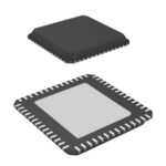 HV2809K6-G-M937

The activity of extra discounts on wholesale prices is in full swing…
Please fill in your contact information and we will send you the latest wholesale price list.





