 ChipApex | Global Electronic Components Supplier

SEARCH
Search Product
Search Post
— IC芯片 | 连接器 | 传感器 | 被动器件 —
Search productSearch post
— IC芯片 | 连接器 | 传感器 | 被动器件 —
Consult the customer manager about the wholesale price.
consultation hotline:86-132-6715-2157
email:[email protected]
Contact the product manager for consultation. One-stop consultation is available.
Do you want a lower wholesale price? Please send us your inquiry and we will reply immediately.
HV582GA-G is listed in the Shift Registers range at ChipApex. The manufacturer field lists Microchip Technology. Its product description is IC 96BIT SHIFT REGISTER 169TFBGA. Review the specifications below when checking this part for your BOM.
The HV582GA-G is a unipolar, 96-channel low-voltage serial to high-voltage parallel converter with push-pull outputs. It features six parallel 16-bit shift registers and a 96-bit latch. The device operates at a data clock frequency of 30 MHz, enabling an effective data rate of 180 MHz due to the parallel arrangement. High-voltage supply (VPP) ranges from 10 V to 80 V, supporting up to 75 mA peak output sink/source current. Logic supply voltage (VDD) is 4.5 V to 5.5 V. It is housed in a 169-ball TFBGA package measuring 10 x 10 x 1.1 mm.
Verify component authenticity through authorized Microchip Technology distributors or direct factory channels. Confirm RoHS compliance status and check for recent Product Change Notifications (PCN) regarding packaging or material updates. Ensure ESD precautions are strictly followed during handling, as the device is sensitive to electrostatic discharge. Validate that the specific ordering suffix matches the required TFBGA package configuration.
Select this component when designing systems requiring multiple high-voltage outputs with significant current drive capabilities. It is suitable for applications needing fast parallel data conversion from serial inputs. Consider the 169-ball TFBGA package constraints for PCB layout. Evaluate thermal management requirements given the operating junction temperature range and power dissipation characteristics under maximum load conditions.
The HV582GA-G belongs to Microchip's HV58x family of serial-to-parallel logic converters. It is functionally related to the HV583, which offers 128 channels. Unlike some lower-channel variants, this part integrates six independent shift registers for enhanced throughput. It serves as a bridge between low-voltage digital logic and high-voltage actuator or display loads.
HV583: Offers 128 channels instead of 96; verify pin compatibility and channel count requirements.
The DIR pin controls the direction of input data flow for the shift registers. When set High, data flows counter-clockwise (DnB to DnA); when Low, it flows clockwise (DnA to DnB).
The Output Low (OL) pin forces all high-voltage outputs to a Low-level state (HVGND), while the Output High (OH) pin forces them to a High-level state (VPP), overriding stored latch data when OE is active.
Explore related parts through Logic, Integrated Circuits (ICs), all product categories, ChipApex homepage.
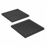 HV582GA-G

The activity of extra discounts on wholesale prices is in full swing…
Please fill in your contact information and we will send you the latest wholesale price list.





