 ChipApex | Global Electronic Components Supplier

SEARCH
Search Product
Search Post
— IC芯片 | 连接器 | 传感器 | 被动器件 —
Search productSearch post
— IC芯片 | 连接器 | 传感器 | 被动器件 —
Consult the customer manager about the wholesale price.
consultation hotline:86-132-6715-2157
email:[email protected]
Contact the product manager for consultation. One-stop consultation is available.
Do you want a lower wholesale price? Please send us your inquiry and we will reply immediately.
HV7620PG-G is listed in the Shift Registers range at ChipApex. The manufacturer field lists Microchip Technology. Its product description is IC 32BIT SRL CMOS 64QFP. Review the specifications below when checking this part for your BOM.
The HV7620PG-G is a low-voltage serial to high-voltage parallel converter with push-pull outputs, designed for color AC plasma displays. It utilizes HVCMOS technology and operates on a 5.0V logic supply (VDD1) and a 12V supply rail (VDD2). The device provides output voltages up to +200V via the VPP pin. It features four parallel 8-bit shift registers allowing data rates of up to 40MHz equivalent. Key electrical parameters include a minimum source/sink current of 50mA, a clock frequency of 10MHz at VDD1=5.0V, and an operating temperature range from -40°C to +85°C.
Verify that the ordering suffix PG-G indicates a lead-free and RoHS compliant package. Confirm the specific datasheet version C112213 matches your design requirements. Ensure power-up sequencing follows the recommended order: Ground, VDD1, VDD2, VPP, then Logic Signals. Check humidity sensitivity handling during assembly as indicated in standard Microchip packaging guidelines.
Select this component when driving color AC plasma displays requiring high-voltage push-pull outputs. It is suitable for systems needing 32-channel parallel output from a serial interface. Consider the 40MHz equivalent data rate and 50mA output current capabilities. Ensure the application supports the required VPP voltage up to 200V and the specified logic supply ranges.
The HV7620 is part of the Supertex Inc. product line, now under Microchip Technology. It belongs to the category of display drivers and controllers, specifically functioning as a serial-to-parallel converter. The device is housed in a 64-Lead PQFP package. It is distinct from other HV series parts by its specific focus on AC plasma display driving with high-voltage push-pull outputs.
Public confirmed substitute part numbers are not available in the provided documentation. Verify compatibility with existing circuit designs if considering alternative components from the same family or manufacturer.
The device supports output voltages up to +200V via the VPP supply pin.
Connecting DIR to VDD1 causes clockwise (CW) shifting, while connecting it to LVGND causes counterclockwise (CCW) shifting.
The recommended sequence is: 1. GND, 2. VDD1, 3. VDD2, 4. VPP, 5. Logic Input Signals.
Explore related parts through Logic, Integrated Circuits (ICs), all product categories, ChipApex homepage.
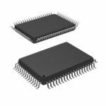 HV7620PG-G

The activity of extra discounts on wholesale prices is in full swing…
Please fill in your contact information and we will send you the latest wholesale price list.




