ChipApex | Global Electronic Components Supplier

SEARCH
Search Product
Search Post
— IC芯片 | 连接器 | 传感器 | 被动器件 —
Search productSearch post
— IC芯片 | 连接器 | 传感器 | 被动器件 —
Consult the customer manager about the wholesale price.
consultation hotline:86-132-6715-2157
email:[email protected]
Contact the product manager for consultation. One-stop consultation is available.
Do you want a lower wholesale price? Please send us your inquiry and we will reply immediately.
The ICL7611DESA+ is a single-channel, low-power monolithic CMOS operational amplifier manufactured by Analog Devices Inc./Maxim Integrated. It operates within a supply voltage range of ±1V to ±8V or 2V to 16V single supply. Key electrical parameters include a typical input bias current of 1pA (max 4nA at +125°C), an input offset voltage of 15mV, and a unity-gain bandwidth of 0.044MHz at the lowest quiescent current setting. The device features programmable quiescent currents of 10μA, 100μA, or 1000μA per amplifier, allowing optimization for power consumption versus speed.
Verify the specific suffix 'DESA+' against the manufacturer's official ordering information to confirm the package type, temperature range, and RoHS compliance status. Confirm availability through authorized distributors as production status may vary. Ensure the selected variant matches the required quiescent current configuration for the target application.
Select this component when ultra-low input bias current and low power consumption are critical requirements. The programmable IQ feature allows designers to optimize the trade-off between bandwidth/slew rate and power dissipation. Verify that the 15mV maximum input offset voltage meets the precision requirements of the specific circuit application.
This part belongs to the ICL761X–ICL764X family of single/dual/triple/quad operational amplifiers. The family is characterized by its monolithic CMOS construction, which enables the combination of extremely low input currents with wide supply voltage operation. The ICL7611 specifically denotes the single-channel version of this architecture.
The datasheet identifies the device as having an industry-standard pinout and being a second source for similar architectures. Cross-reference with other manufacturers offering pin-compatible CMOS op-amps with comparable bias current specifications if sourcing is restricted.
For the ICL7611, the quiescent current is programmable via the IQ pin. Connecting the IQ pin to V+ selects 10μA, connecting it between V- + 0.8V and V+ - 0.8V selects 100μA, and connecting it to V- selects 1000μA.
Yes, the input offset can be nulled by connecting a 25kΩ potentiometer between the OFFSET terminals with the wiper connected to V+. This method is effective at quiescent currents of 100μA and 1mA.
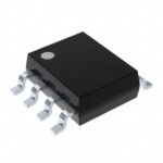 ICL7611DESA+

The activity of extra discounts on wholesale prices is in full swing…
Please fill in your contact information and we will send you the latest wholesale price list.