 ChipApex | Global Electronic Components Supplier
SEARCH
Search Product
Search Post
— IC芯片 | 连接器 | 传感器 | 被动器件 —
Search productSearch post
— IC芯片 | 连接器 | 传感器 | 被动器件 —
Consult the customer manager about the wholesale price.
consultation hotline:86-132-6715-2157
email:[email protected]
Contact the product manager for consultation. One-stop consultation is available.
Do you want a lower wholesale price? Please send us your inquiry and we will reply immediately.
The ICS557G-03T is a spread spectrum clock generator designed for PCI Express Gen 1 and Ethernet applications. It features a single Phase-Locked Loop (PLL) circuit with a 1:2 input-to-output ratio, accepting a 25 MHz crystal or clock input. The device provides two differential outputs supporting HCSL or LVDS signaling levels. Operating on a 3.3 V supply (2.97V to 3.63V), it generates output frequencies of 25 MHz, 100 MHz, 125 MHz, or 200 MHz for HCSL, and up to 100 MHz for LVDS. Packaged in a 16-TSSOP, it exhibits a cycle-to-cycle jitter of 80 ps and operates within the commercial temperature range of 0°C to +70°C.
Verify the ordering suffix 'T' corresponds to Tape and Reel packaging as specified in the datasheet. Confirm RoHS compliance status by checking for the 'LF' suffix if lead-free material is required. Ensure the component meets the commercial temperature range specifications of 0°C to +70°C for the intended application environment.
Select this component when a 1:2 fanout with spread spectrum is required for PCIe Gen 1. Choose the HCSL configuration for standard PCI Express layouts or LVDS if specific voltage level compatibility is needed. Verify that the 25 MHz input frequency matches the system crystal oscillator. Consider the industrial variant (ICS557GI-03T) if operation below 0°C is necessary.
The ICS557G-03T belongs to the ICS557-03 family of PCI Express Gen 1 clock sources manufactured by Renesas Electronics (formerly IDT). It serves as a specialized timing solution for reducing electromagnetic interference in high-speed digital interfaces. The 'G' suffix typically denotes the commercial temperature grade, while 'T' indicates tape and reel shipping.
For PCIe Gen 2 applications, consider the 5V41065. For PCIe Gen 3 applications, consider the 5V41235. Direct functional replacements within the same package and pinout should be verified against the specific output frequency and jitter requirements of the design.
Output frequencies (25, 100, 125, or 200 MHz for HCSL) are selected using the S0 and S1 input pins according to the Output Select Table in the datasheet.
The spread spectrum modulation frequency is typically 30 kHz to 33 kHz, with a center frequency of 31.5 kHz.
Yes, the X1/ICLK pin accepts either a 25 MHz fundamental mode parallel resonant crystal or a single-ended LVCMOS clock input.
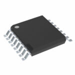 ICS557G-03T
The activity of extra discounts on wholesale prices is in full swing…
Please fill in your contact information and we will send you the latest wholesale price list.






