 ChipApex | Global Electronic Components Supplier
SEARCH
Search Product
Search Post
— IC芯片 | 连接器 | 传感器 | 被动器件 —
Search productSearch post
— IC芯片 | 连接器 | 传感器 | 被动器件 —
Consult the customer manager about the wholesale price.
consultation hotline:86-132-6715-2157
email:[email protected]
Contact the product manager for consultation. One-stop consultation is available.
Do you want a lower wholesale price? Please send us your inquiry and we will reply immediately.
The ICS557G-08T is a 2:1 multiplexer chip designed for PCI Express applications, manufactured by Renesas Electronics Corporation. It allows the selection of one of two HCSL or LVDS input pairs and fans out to one pair of differential outputs. The device operates at a maximum frequency of 200 MHz with an HCSL termination and up to 100 MHz with LVDS termination. It functions within a supply voltage range of 3.135V to 3.465V and supports commercial temperature operation from 0°C to +70°C. Packaged in a 16-pin TSSOP (0.173" width), it provides low power consumption and requires minimal external components.
Verify the specific ordering suffix to confirm package type and temperature range. The 'T' suffix indicates tape and reel packaging. Ensure compatibility with the required operating temperature range, as non-industrial variants are limited to 0°C to +70°C. Confirm RoHS compliance status based on the 'LF' suffix if lead-free material is required for the assembly process.
Select this component when a single-ended or differential clock source needs to be switched between two inputs for a PCI Express system. Verify that the input signal levels match the HCSL or LVDS requirements. Ensure the PCB layout accommodates the 16-pin TSSOP footprint and includes necessary decoupling capacitors close to the VDD pins for optimal performance.
This part belongs to the ICS557 series of PCI Express clock multiplexers. It is distinct from clock generators like the 557GI-05ALFT, which produce clocks rather than selecting them. The 'G' suffix typically denotes the standard commercial temperature grade, differentiating it from the 'I' grade industrial variant.
Direct replacements include other parts from the ICS557 family, such as the ICS557G-08LF for tube packaging or the ICS557GI-08T for industrial temperature ranges. Cross-vendor equivalents should be verified against the 2:1 mux topology and PCIe signaling standards.
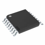 ICS557G-08T
The activity of extra discounts on wholesale prices is in full swing…
Please fill in your contact information and we will send you the latest wholesale price list.





