 ChipApex | Global Electronic Components Supplier
SEARCH
Search Product
Search Post
— IC芯片 | 连接器 | 传感器 | 被动器件 —
Search productSearch post
— IC芯片 | 连接器 | 传感器 | 被动器件 —
Consult the customer manager about the wholesale price.
consultation hotline:86-132-6715-2157
email:[email protected]
Contact the product manager for consultation. One-stop consultation is available.
Do you want a lower wholesale price? Please send us your inquiry and we will reply immediately.
The ICS557GI-06 is a two-to-four differential clock multiplexer designed for PCI Express applications. It selects one of two differential HCSL or LVDS input pairs and fans out to four pairs of differential outputs. The device operates at a supply voltage of 3.135V to 3.465V with a maximum frequency of 200 MHz for HCSL and 100 MHz for LVDS. Key electrical parameters include a cycle-to-cycle jitter of 60 ps, an output-to-output skew of 50 ps, and an operating temperature range of -40°C to +85°C.
Verify the specific ordering suffix to confirm package type and temperature rating. The 'LF' suffix indicates lead-free packaging compliant with RoHS standards. The 'I' suffix denotes the industrial temperature range (-40°C to +85°C). Confirm availability as non-green parts may have reached end-of-life status.
Select this component when a 2:4 fan-out buffer is required for PCIe designs. Ensure the input source matches the supported HCSL or LVDS levels. Verify that the external termination resistors align with the specified 50 ohm trace impedance requirements for optimal signal integrity.
This part belongs to the ICS557 series of clock buffers and muxes from Integrated Device Technology (IDT), now part of Renesas Electronics. It serves as a fan-out buffer solution for high-speed serial interfaces like PCI Express Gen 1.
Direct replacements include the ICS557G-06 (commercial temperature) or ICS557GI-06LF (industrial temperature, tape and reel). Verify pin compatibility and electrical specifications before substitution.
The maximum input frequency for LVDS signals is 100 MHz.
Input selection is controlled by the SEL pin; SEL=1 selects IN1/IN1, while SEL=0 selects IN2/IN2.
When the PD pin is low, the chip powers down and tri-states the outputs.
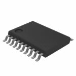 ICS557GI-06
The activity of extra discounts on wholesale prices is in full swing…
Please fill in your contact information and we will send you the latest wholesale price list.






