 ChipApex | Global Electronic Components Supplier
SEARCH
Search Product
Search Post
— IC芯片 | 连接器 | 传感器 | 被动器件 —
Search productSearch post
— IC芯片 | 连接器 | 传感器 | 被动器件 —
Consult the customer manager about the wholesale price.
consultation hotline:86-132-6715-2157
email:[email protected]
Contact the product manager for consultation. One-stop consultation is available.
Do you want a lower wholesale price? Please send us your inquiry and we will reply immediately.
The ICS557M-01T is a clock generator designed for PCI Express applications, manufactured by Renesas Electronics Corporation. It utilizes a Phase-Locked Loop (PLL) to convert a 25 MHz crystal input into a 100 MHz differential output. The device supports HCSL and LVDS signaling levels within an 8-pin SOIC package. Key electrical parameters include a supply voltage range of 3.135V to 3.465V, a maximum operating temperature of +70°C, and short-term jitter of 100 ps peak-to-peak. It consumes 55 mA at full load.
Verify the 'T' suffix indicates tape and reel packaging rather than tube. Confirm RoHS compliance status, as non-green parts have reached end-of-life. Ensure the commercial temperature grade (+70°C max) meets system requirements instead of the industrial variant.
Select this component when a single-ended 25 MHz crystal must drive a 100 MHz PCIe interface. Compare against the ICS557MI-01T if an extended -40°C to +85°C temperature range is required. Verify that the 8-pin SOIC footprint fits the PCB layout constraints.
This part belongs to the ICS557 series of PCI Express clock sources. It serves as a foundational timing component for Gen1 PCIe designs. Related models in the family include the ICS557-03 for dual outputs and higher frequency support.
ICS557MI-01T: Industrial temperature version (-40°C to +85°C).
The OE pin controls the output state. A high logic level enables the differential outputs, while a low logic level tristates them.
A 25 MHz fundamental mode parallel resonant crystal with a 16 pF load capacitance is required. External capacitors should be calculated based on the formula CL = (Cload - 8) * 2.
Yes, LVDS signal levels can be supported via an alternative termination scheme using specific resistor values (RP, RQ, RT) as detailed in the datasheet guidelines.
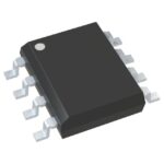 ICS557M-01T
The activity of extra discounts on wholesale prices is in full swing…
Please fill in your contact information and we will send you the latest wholesale price list.





