 ChipApex | Global Electronic Components Supplier

SEARCH
Search Product
Search Post
— IC芯片 | 连接器 | 传感器 | 被动器件 —
Search productSearch post
— IC芯片 | 连接器 | 传感器 | 被动器件 —
Consult the customer manager about the wholesale price.
consultation hotline:86-132-6715-2157
email:[email protected]
Contact the product manager for consultation. One-stop consultation is available.
Do you want a lower wholesale price? Please send us your inquiry and we will reply immediately.
ICS651M is listed in the Clock Buffers, Drivers range at ChipApex. The manufacturer field lists Renesas Electronics Corporation. Its product description is IC CLK BUFFER 1:4 200MHZ 8SOIC. Review the specifications below when checking this part for your BOM.
The ICS651M is a low skew, single-input to four-output LVCMOS clock buffer from the Renesas 621S series. It features sub-50fs RMS additive phase jitter and supports input frequencies up to 200 MHz. The device operates on a supply voltage range of 1.71 V to 3.465 V, typically covering 1.8 V to 3.3 V applications. It exhibits a maximum propagation delay of 4.5 ns and functions within an industrial temperature range of -40°C to +105°C. Packaged in an 8-pin CMG format with a 0.5 mm pitch, it is designed for high-speed timing distribution.
Verify the specific suffix 'M' against official Renesas documentation to confirm package type and tape/reel specifications. Confirm RoHS compliance status directly with the manufacturer or authorized distributors, as regulatory details may vary by production batch. Ensure the ordering part number matches the required lead count and moisture sensitivity level (MSL 1) for your assembly process.
Select this component when sub-50fs jitter performance is critical for signal integrity. Verify that the system power supply remains stable within the 1.71 V to 3.465 V range to ensure correct logic levels. Consider the 4.5 ns propagation delay for timing budget calculations in high-frequency designs requiring precise clock alignment across multiple loads.
The ICS651M belongs to the Renesas 621S family of clock buffers. This series is engineered for cost-effective, high-speed timing solutions using LVCMOS outputs. It serves as a direct replacement for legacy ICSClock products, maintaining compatibility with standard digital interfaces while offering improved jitter characteristics for modern high-bandwidth applications.
Consult official substitution guides for equivalent parts within the 621S family. Verify pinout compatibility and electrical parameters before replacing existing designs with alternative manufacturers' components.
Explore related parts through Clock/Timing, Integrated Circuits (ICs), all product categories, ChipApex homepage.
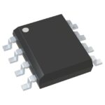 ICS651M

The activity of extra discounts on wholesale prices is in full swing…
Please fill in your contact information and we will send you the latest wholesale price list.




