 ChipApex | Global Electronic Components Supplier

SEARCH
Search Product
Search Post
— IC芯片 | 连接器 | 传感器 | 被动器件 —
Search productSearch post
— IC芯片 | 连接器 | 传感器 | 被动器件 —
Consult the customer manager about the wholesale price.
consultation hotline:86-132-6715-2157
email:[email protected]
Contact the product manager for consultation. One-stop consultation is available.
Do you want a lower wholesale price? Please send us your inquiry and we will reply immediately.
ICS853111BYLF is listed in the Clock Buffers, Drivers range at ChipApex. The manufacturer field lists Renesas Electronics Corporation. Its product description is IC CLK BUFFER 2:10 3GHZ 32TQFP. Review the specifications below when checking this part for your BOM.
The ICS853111BYLF is a low skew, high performance 1-to-10 differential-to-2.5V/3.3V LVPECL/ECL fanout buffer from the HiPerClockS family. It features ten differential outputs and two selectable differential input pairs (PCLKx/nPCLKx) supporting LVPECL, LVDS, CML, and SSTL levels. The device operates with a maximum output frequency exceeding 3GHz. Key electrical parameters include a typical propagation delay of 495ps, output skew of 20ps, part-to-part skew of 85ps, and RMS additive phase jitter under 0.03ps. It supports LVPECL mode (VCC = 2.375V to 3.8V, VEE = 0V) and ECL mode (VCC = 0V, VEE = -3.8V to -2.375V) within an ambient operating temperature range of -40°C to 85°C.
Verify RoHS compliance status for the specific ordering suffix, as the datasheet indicates availability in both standard (RoHS 5) and lead-free (RoHS 6) packages. Confirm package type Y (32-Lead TQFP, E-PAD) matches design requirements. Check current manufacturing status and lifecycle stage through authorized distributors or Renesas Electronics, as IDT products may have transitioned statuses.
Select this component when a 1-to-10 fanout ratio with sub-nanosecond propagation delay is required. Ensure the system power supply aligns with either the 2.5V or 3.3V LVPECL mode ranges. Verify that the input source signal levels (LVPECL, LVDS, CML, SSTL) are compatible with the PCLKx/nPCLKx inputs. Consider thermal management for the 32-lead TQFP package if multiple outputs are loaded, as total power dissipation increases with active loads.
The ICS853111B belongs to the HiPerClockS family of high-performance clock solutions originally developed by Integrated Device Technology (IDT), which was acquired by Renesas Electronics. This series is designed for applications demanding low skew and high repeatability in clock distribution networks.
The datasheet notes pin compatibility with MC100EP111 and MC100LVEP111. Verify functional equivalence and electrical specifications before substitution.
Yes, the device can translate any single-ended input signal to 3.3V LVPECL levels by applying resistor bias on the nPCLK input.
The maximum output frequency is specified as greater than 3GHz.
Setting CLK_SEL to logic high selects the PCLK1/nPCLK1 input pair, while setting it to logic low selects the PCLK0/nPCLK0 input pair.
Explore related parts through Clock/Timing, Integrated Circuits (ICs), all product categories, ChipApex homepage.
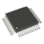 ICS853111BYLF

The activity of extra discounts on wholesale prices is in full swing…
Please fill in your contact information and we will send you the latest wholesale price list.






