 ChipApex | Global Electronic Components Supplier
SEARCH
Search Product
Search Post
— IC芯片 | 连接器 | 传感器 | 被动器件 —
Search productSearch post
— IC芯片 | 连接器 | 传感器 | 被动器件 —
Consult the customer manager about the wholesale price.
consultation hotline:86-132-6715-2157
email:[email protected]
Contact the product manager for consultation. One-stop consultation is available.
Do you want a lower wholesale price? Please send us your inquiry and we will reply immediately.
The ICS9FG108DFILF is a clock frequency timing generator manufactured by Renesas Electronics Corporation. It features a single PLL circuit with one input and nine outputs, providing a 1:9 ratio. The device supports HCSL output signaling and accepts crystal or clock inputs. It operates within a supply voltage range of 3.135V to 3.465V and achieves a maximum frequency of 400MHz. Designed for surface mount installation, it is housed in a 48-BSSOP package (0.295" width) and functions reliably across an extended temperature range of -40°C to +85°C.
Verify the specific suffix 'DF' against official Renesas documentation to confirm pinout compatibility and electrical characteristics relative to other variants in the 9FG108 series. Ensure the 48-BSSOP footprint matches the target PCB design. Confirm RoHS compliance status through the manufacturer's current product compliance reports before finalizing procurement specifications.
Select this component when a 1:9 clock distribution ratio is required for Intel server architectures or high-speed serial interfaces like PCIe and SATA. The -40°C to +85°C rating makes it suitable for industrial environments. Compare against the 9FG108EGLF if a commercial temperature range (0°C to 70°C) suffices, as the DF variant offers broader thermal coverage.
This part belongs to the 9FG108 family of clock synthesizers designed for data communications. It serves as a jitter cleaner and frequency multiplier for critical system buses. The device integrates a phase-locked loop to generate stable clock signals from a reference crystal or external clock source, ensuring signal integrity for downstream logic components.
Publicly confirmed substitute part numbers are not available in the provided source material. Cross-referencing with the 9FG108EGLF requires verification of temperature range differences and package pinout compatibility.
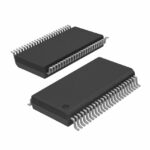 ICS9FG108DFILF
The activity of extra discounts on wholesale prices is in full swing…
Please fill in your contact information and we will send you the latest wholesale price list.






