 ChipApex | Global Electronic Components Supplier
SEARCH
Search Product
Search Post
— IC芯片 | 连接器 | 传感器 | 被动器件 —
Search productSearch post
— IC芯片 | 连接器 | 传感器 | 被动器件 —
Consult the customer manager about the wholesale price.
consultation hotline:86-132-6715-2157
email:[email protected]
Contact the product manager for consultation. One-stop consultation is available.
Do you want a lower wholesale price? Please send us your inquiry and we will reply immediately.
The ICS9P946AFLFT is a dedicated clock buffer integrated circuit manufactured by Renesas Electronics Corporation. Designed for memory subsystems, specifically DDR and DDR2 applications, this device operates with a maximum frequency of 533 MHz. It features two independent circuits configured with a 1:6 input-to-output ratio. The component supports differential signaling on both the input and output sides, ensuring signal integrity in high-speed digital environments. It functions within a supply voltage range of 3.3V and is rated for an operating temperature range of 0°C to 70°C.
Verify the package designation matches the 48-BSSOP (7.50mm width) specification. Confirm that the 3.3V supply requirement aligns with the target system's power rails. Ensure the operating temperature range of 0°C to 70°C meets the environmental constraints of the final assembly. Cross-reference the manufacturer part number with Renesas documentation to confirm current production status.
Select this component when a 1:6 fan-out is required for DDR/DDR2 memory buses. The differential I/O capability makes it suitable for noise-sensitive environments. Ensure the design accommodates the 3.3V logic levels. Compare against other clock buffers if lower pin counts or different voltage supplies are needed. Verify that the 533 MHz speed grade satisfies the memory controller's requirements.
This component belongs to the Application Specific Clock/Timing category. It serves as a specialized buffer rather than a general-purpose oscillator or PLL-based generator. Its primary role is to distribute reference clocks to multiple memory devices while maintaining signal quality and timing alignment in computer and communication hardware.
Check for direct pin-compatible alternatives from Renesas with identical 48-SSOP packaging. Verify that any substitute maintains the 1:6 ratio and differential I/O characteristics. Ensure the replacement supports the same 3.3V supply and 533 MHz frequency limit.
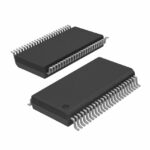 ICS9P946AFLFT
The activity of extra discounts on wholesale prices is in full swing…
Please fill in your contact information and we will send you the latest wholesale price list.





