 ChipApex | Global Electronic Components Supplier

SEARCH
Search Product
Search Post
— IC芯片 | 连接器 | 传感器 | 被动器件 —
Search productSearch post
— IC芯片 | 连接器 | 传感器 | 被动器件 —
Consult the customer manager about the wholesale price.
consultation hotline:86-132-6715-2157
email:[email protected]
Contact the product manager for consultation. One-stop consultation is available.
Do you want a lower wholesale price? Please send us your inquiry and we will reply immediately.
IDT23S09E-1DCI8 is listed in the Clock Generators, PLLs, Frequency Synthesizers range at ChipApex. The manufacturer field lists Renesas Electronics Corporation. Its product description is IC ZD BUFFER 16SOIC. Review the specifications below when checking this part for your BOM.
The IDT23S09E-1DCI8 is a 3.3V zero delay clock buffer manufactured by Renesas Electronics Corporation, originally developed by Integrated Device Technology (IDT). It features an internal phase-lock loop (PLL) that aligns the phase between the incoming reference clock and output clocks, achieving zero I/O delay. The device distributes one clock input to two banks of outputs: Bank A comprises four pins (CLKA1–4), and Bank B comprises four pins (CLKB1–4), with an additional CLKOUT pin used for internal PLL feedback. It operates within a frequency range of 10MHz to 200MHz at a 3.3V supply voltage.
Verify the ordering suffix 'I' confirms the Industrial temperature range (-40°C to +85°C). Confirm the 'DC' suffix indicates the standard drive version in a 16-pin SOIC package. Check for RoHS compliance status as non-green parts had an end-of-life date of May 13, 2010.
Select this component when a 3.3V zero delay buffer with 1:8 distribution is required. Ensure the load capacitance matches the operating frequency (<30pF for <100MHz, <10pF for 100-200MHz). For true zero delay, all outputs including CLKOUT must be equally loaded.
This part belongs to the IDT23S09E series, which includes variants like the -1H (High Drive) and different packaging options such as TSSOP. It is a 16-pin version derived from the IDT23S05E family. The manufacturer transitioned from IDT to Renesas Electronics Corporation.
Public confirmed substitute part numbers are not available in the provided documentation. Consider checking for IDT23S09E-1HDCI8 if higher drive strength is needed, or IDT23S09E-1DCG/PG variants for alternative packages.
Zero delay is achieved by aligning the phase between the incoming clock and the output clock using the internal PLL. The CLKOUT pin provides the feedback signal for the PLL.
In the absence of an input clock, the device enters power down mode. The outputs become tri-stated, and current draw drops below 25µA for the industrial temperature range.
Yes, the IDT23S09E is designed to be spread spectrum compatible and will not filter off the spread spectrum feature of the reference input.
Explore related parts through Clock/Timing, Integrated Circuits (ICs), all product categories, ChipApex homepage.
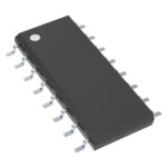 IDT23S09E-1DCI8

The activity of extra discounts on wholesale prices is in full swing…
Please fill in your contact information and we will send you the latest wholesale price list.







