 ChipApex | Global Electronic Components Supplier
SEARCH
Search Product
Search Post
— IC芯片 | 连接器 | 传感器 | 被动器件 —
Search productSearch post
— IC芯片 | 连接器 | 传感器 | 被动器件 —
Consult the customer manager about the wholesale price.
consultation hotline:86-132-6715-2157
email:[email protected]
Contact the product manager for consultation. One-stop consultation is available.
Do you want a lower wholesale price? Please send us your inquiry and we will reply immediately.
The IDT5T929-30NLGI is a precision clock generator designed for OC-48 SONET/SDH applications. It generates high-precision FEC or non-FEC source clocks and supports Gigabit Ethernet systems. The device features hitless switchover between two redundant inputs (CLKIN and REFIN) to maintain output continuity during input failure. It accepts differential LVPECL, LVDS, or single-ended LVTTL inputs and provides LVPECL outputs. Operating on a 2.375V to 3.465V supply, it functions within an industrial temperature range of -40°C to +85°C.
This component has been discontinued by the manufacturer. The last time buy expired on October 28, 2014. Verification of current availability requires checking secondary market distributors or authorized surplus suppliers, as original factory stock is no longer active.
Select the IDT5T929-30NLGI specifically for LVPECL output requirements; the -10 variant offers LVDS outputs. Ensure the system design accommodates the 28-VFQFPN (6x6 mm) package dimensions. Verify that the required input frequencies align with the supported SONET, FEC, or 10GE standards listed in the datasheet specifications.
The IDT5T929 belongs to the IDT precision clock generator family, originally manufactured by Integrated Device Technology, Inc., which was acquired by Renesas Electronics Corporation. This specific part targets high-speed telecommunications infrastructure requiring precise timing synchronization for OC-48 rates.
The datasheet explicitly identifies the 8T49N222B-dddNLGI as a replacement part for this device. Designers should evaluate the electrical compatibility and pinout differences when transitioning to this alternative.
The device utilizes a hitless switchover mechanism. If CLKIN fails, the PLL smoothly switches to lock onto the REFIN input without generating glitches on the output. A LOCK indicator pin signals the switch status.
The IDT5T929 supports differential LVPECL, differential LVDS, and single-ended LVTTL input interfaces. Single-ended inputs can be used by connecting one side of the differential pair to ground via a capacitor if the other is left floating.
QREG provides a regenerated version of the input clock signal. It squares up the rising and falling edges of the input clock using the internal oscillator to remove jitter, regardless of whether the device is locked to CLKIN or REFIN.
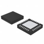 IDT5T929-30NLGI
The activity of extra discounts on wholesale prices is in full swing…
Please fill in your contact information and we will send you the latest wholesale price list.






