 ChipApex | Global Electronic Components Supplier

SEARCH
Search Product
Search Post
— IC芯片 | 连接器 | 传感器 | 被动器件 —
Search productSearch post
— IC芯片 | 连接器 | 传感器 | 被动器件 —
Consult the customer manager about the wholesale price.
consultation hotline:86-132-6715-2157
email:[email protected]
Contact the product manager for consultation. One-stop consultation is available.
Do you want a lower wholesale price? Please send us your inquiry and we will reply immediately.
IDT71P71804S250BQ is listed in the Memory IC range at ChipApex. The manufacturer field lists Renesas Electronics Corporation. Its product description is IC SRAM 18MBIT PAR 165CABGA. Review the specifications below when checking this part for your BOM.
The IDT71P71804S250BQ is an 18Mb synchronous DDR II SRAM with a 1M x 18 organization. It features a common bidirectional data port and multiplexed address bus, supporting two-word bursts per clock cycle. The device operates at a maximum clock frequency of 250 MHz with a 6.3 ns access time. It utilizes a 165-ball CABGA package measuring 13mm x 15mm. Core voltage (VDD) ranges from 1.7V to 1.9V, while I/O supply (VDDQ) scales from 1.4V to 1.9V. Operating temperature is specified from 0°C to +70°C.
Verify the specific speed grade suffix matches the required clock frequency, as the base part number covers multiple variants. Confirm that the 165-CABGA footprint aligns with the target PCB design. Ensure power delivery supports the 1.8V core and scalable VDDQ requirements. Check for RoHS compliance status if environmental regulations apply to the end product.
Select this component when a high-bandwidth, low-latency memory solution with a wide data bus is required. The 1M x 18 configuration suits applications needing parallel data paths. Consider the programmable impedance feature for signal integrity optimization in complex board layouts. Verify compatibility with HSTL or scaled voltage interfaces for the host controller.
This device belongs to the IDT71P71 family of DDR II Burst of Two SRAMs. Other members include the IDT71P71204 (2Mx8), IDT71P71104 (2Mx9), and IDT71P71604 (512Kx36). All share similar architectural features but differ in bit-width and depth configurations within the same 165-ball package.
Public confirmed substitute part numbers are not available in the provided documentation. Consult manufacturer resources for obsolescence management or cross-reference alternatives based on pinout and electrical specifications.
An external resistor (RQ) connects the ZQ pin to ground. The output impedance is set to 0.2 times the RQ value, allowing adjustment between 35 ohms and 70 ohms.
SA0 serves as a burst count address bit, allowing the user to reverse the burst order or address individual words within a burst during read or write operations.
Explore related parts through Memory, Integrated Circuits (ICs), all product categories, ChipApex homepage.
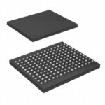 IDT71P71804S250BQ

The activity of extra discounts on wholesale prices is in full swing…
Please fill in your contact information and we will send you the latest wholesale price list.





