 ChipApex | Global Electronic Components Supplier

SEARCH
Search Product
Search Post
— IC芯片 | 连接器 | 传感器 | 被动器件 —
Search productSearch post
— IC芯片 | 连接器 | 传感器 | 被动器件 —
Consult the customer manager about the wholesale price.
consultation hotline:86-132-6715-2157
email:[email protected]
Contact the product manager for consultation. One-stop consultation is available.
Do you want a lower wholesale price? Please send us your inquiry and we will reply immediately.
IDT71V3577S85PF8 is listed in the Memory IC range at ChipApex. The manufacturer field lists Renesas Electronics Corporation. Its product description is IC SRAM 4.5MBIT PARALLEL 100TQFP. Review the specifications below when checking this part for your BOM.
The IDT71V3577S85PF8 is a high-speed synchronous static random access memory (SRAM) manufactured by Renesas Electronics Corporation. It features a memory organization of 128K x 36 bits, providing a total capacity of 4.5 Mbit. The device operates with a maximum clock frequency of 87 MHz and supports an access time of 8.5 ns. It utilizes a parallel interface and requires a core supply voltage range of 3.135 V to 3.465 V. The component is housed in a 100-pin thin quad flatpack (TQFP) package.
Verify the specific suffix PF8 against official Renesas documentation to confirm package type and temperature grade. Confirm RoHS compliance status as historical records vary. Check current lifecycle status as this series may be discontinued or subject to last-time buy notices. Ensure compatibility with existing board layouts for the 100-pin TQFP footprint.
Select this component when a 128K x 36 organization is required for synchronous applications. The 8.5 ns speed grade suits designs operating up to 87 MHz. Consider the flow-through output characteristic if low latency is critical compared to registered outputs. Verify that the 3.3V I/O levels match the system bus requirements.
This part belongs to the IDT71V3577/79 family of 3.3V synchronous SRAMs. The 'S' suffix typically denotes commercial temperature range operation. The family includes variants with different densities and speeds, such as the 7.5 ns and 8.0 ns grades. These devices are designed for high-performance embedded memory applications.
Official substitutes include other members of the IDT71V3577 family with compatible speed grades and packages. Cross-vendor replacements require verification of pinout compatibility and electrical characteristics. Consult Renesas PCN documents for end-of-life notifications and approved alternative part numbers.
The 'SA' suffix indicates the inclusion of an optional Boundary Scan JTAG interface compliant with IEEE 1149.1, which is not present in the standard 'S' version.
The LBO pin selects the burst sequence order. A LOW state on LBO selects the linear burst sequence, while a HIGH state selects the interleaved burst sequence.
Explore related parts through Memory, Integrated Circuits (ICs), all product categories, ChipApex homepage.
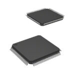 IDT71V3577S85PF8

The activity of extra discounts on wholesale prices is in full swing…
Please fill in your contact information and we will send you the latest wholesale price list.





