 ChipApex | Global Electronic Components Supplier
IDT74LVC541AQG
Search Product
Search Post
— IC芯片 | 连接器 | 传感器 | 被动器件 —
Search productSearch post
— IC芯片 | 连接器 | 传感器 | 被动器件 —
Consult the customer manager about the wholesale price.
consultation hotline:86-132-6715-2157
email:[email protected]
Contact the product manager for consultation. One-stop consultation is available.
Do you want a lower wholesale price? Please send us your inquiry and we will reply immediately.
The IDT74LVC541AQG is an octal buffer and line driver featuring three-state outputs, manufactured using 0.5-micron CMOS technology. It operates within a supply voltage range of 2.7V to 3.6V, with normal operation at 3.3V ± 0.3V. The device provides high output drive capability of ±24mA and features rail-to-rail output swing for improved noise margins. All inputs and outputs are 5V tolerant, allowing compatibility in mixed-voltage systems. It supports hot insertion and includes ESD protection exceeding 2000V per MIL-STD-883 Method 3015.
Verify the specific suffix 'QG' corresponds to the Quarter Size Small Outline Package (QSOP) variant when sourcing. Confirm the temperature grade matches the industrial range specification (-40°C to +85°C). Ensure the ordering code aligns with the non-bus-hold configuration as indicated by the blank designation in the base part number structure.
Select this component for applications requiring high fan-out and strong drive strength on octal buses. The 5V tolerance feature makes it suitable for legacy interface bridging where older 5V logic must communicate with modern 3.3V processors. Consider the QSOP package dimensions if board space constraints favor smaller footprints over standard SOIC packages.
This device belongs to the LVC family of octal buffers, designed for high-speed digital signal buffering. It serves as a bridge between different voltage domains, specifically facilitating data transfer from 5V sources to 3.3V destinations. The design emphasizes low power consumption typical of CMOS technology while delivering sufficient current for bus driving applications.
Compatible substitutes include other octal 3-state buffers with 5V tolerance such as the 74LVC541 series from various manufacturers. Verify pinout compatibility and ensure the replacement package matches the QSOP form factor or requires adapter solutions.
To ensure the high-impedance state during power-up or power-down, the OE inputs should be tied to VCC through a pullup resistor. The minimum resistor value is determined by the current-sinking capability of the driver.
OE1 and OE2 are active-low output enable inputs. If either input is high, all eight outputs enter the high-impedance state. Data transfers from inputs to outputs only when both OE1 and OE2 are low.
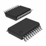 IDT74LVC541AQG
The activity of extra discounts on wholesale prices is in full swing…
Please fill in your contact information and we will send you the latest wholesale price list.





