ChipApex | Global Electronic Components Supplier

SEARCH
Search Product
Search Post
— IC芯片 | 连接器 | 传感器 | 被动器件 —
Search productSearch post
— IC芯片 | 连接器 | 传感器 | 被动器件 —
Consult the customer manager about the wholesale price.
consultation hotline:86-132-6715-2157
email:[email protected]
Contact the product manager for consultation. One-stop consultation is available.
Do you want a lower wholesale price? Please send us your inquiry and we will reply immediately.
The INA190A1NDDFREP is a bidirectional, low-power, zero-drift current sense amplifier from the enhanced product (EP) series. It operates on a single supply voltage ranging from 1.7 V to 5.5 V and supports common-mode voltages from -0.2 V to +40 V. The device features a fixed gain of 25 V/V, a maximum gain error of ±0.2%, and a minimum common-mode rejection ratio of 132 dB. It includes an enable pin that reduces quiescent current to less than 0.1 µA when disabled. The component is housed in an SOT-23-THIN-8 package and is rated for an operating temperature range of -55°C to +150°C.
Verify the specific ordering suffix 'DDFREP' corresponds to the SOT-23-THIN-8 package and tape-and-reel packaging format. Confirm the 'EP' designation indicates the controlled baseline and extended lifecycle status required for defense or aerospace qualification. Ensure the datasheet revision matches the design-in requirements for the -55°C to +150°C temperature range.
Select this variant for applications requiring a 25 V/V gain and operation within the -55°C to +150°C industrial/military temperature range. The low input bias current makes it suitable for high-impedance shunt sensing. Consider the enable pin functionality if system power management requires periodic shutdown. Verify that the 40 V common-mode voltage range aligns with the bus voltage specifications of the target circuit.
This component belongs to the INA190-EP family of current sense amplifiers designed for ruggedized environments. The EP series offers controlled baselines, single assembly/fabrication sites, and extended product change notifications. It shares architectural similarities with standard INA190 devices but is qualified for higher reliability standards and wider temperature extremes.
INA190A1QDCKRQ1G4: Automotive grade alternative with AEC-Q100 qualification and SC-70-6 package.
It utilizes an external reference voltage applied to the REF pin. Positive differential inputs produce outputs above this reference, while negative inputs produce outputs below it.
Driving the ENABLE pin to GND disables the device, reducing the typical supply current to less than 0.1 µA and placing the output in a high-impedance state.
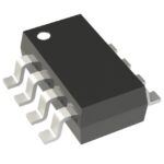 INA190A1NDDFREP

The activity of extra discounts on wholesale prices is in full swing…
Please fill in your contact information and we will send you the latest wholesale price list.