ChipApex | Global Electronic Components Supplier

SEARCH
Search Product
Search Post
— IC芯片 | 连接器 | 传感器 | 被动器件 —
Search productSearch post
— IC芯片 | 连接器 | 传感器 | 被动器件 —
Consult the customer manager about the wholesale price.
consultation hotline:86-132-6715-2157
email:[email protected]
Contact the product manager for consultation. One-stop consultation is available.
Do you want a lower wholesale price? Please send us your inquiry and we will reply immediately.
The INA190A1QDDFRQ1 is an automotive-grade, bidirectional current sense amplifier with a fixed gain of 25 V/V. It operates on a single supply voltage ranging from 1.7 V to 5.5 V and supports common-mode voltages from -0.2 V to +40 V. The device features a maximum offset voltage of ±15 µV and a minimum common-mode rejection ratio of 132 dB. It draws a typical quiescent current of 65 µA when enabled and reduces to 100 nA maximum in shutdown mode. The component is housed in an SOT-23-THIN-8 package and is qualified for operation between -40°C and +125°C.
Verify the specific A1 gain variant matches the design requirement of 25 V/V. Confirm the DDF package includes the ENABLE pin functionality if power management is required. Ensure the operating environment stays within the specified -40°C to +125°C range. Check that the common-mode voltage does not exceed the 40 V limit during transient events.
Select this component for applications requiring precise measurement of microamp-level currents where low input bias current is critical. The fixed 25 V/V gain suits scenarios with small differential signals. Consider the SOT-23-THIN-8 package for space-constrained designs. Verify compatibility with the system's supply voltage range of 1.7 V to 5.5 V.
This part belongs to the INA190-Q1 family of ultra-precise current sense amplifiers designed for automotive environments. It shares the core zero-drift technology and low bias current characteristics with other variants like the INA190A2QDDFRQ1, differing primarily in gain settings and package options. The series is engineered for direct connection to automotive battery rails.
INA190A2QDDFRQ1 offers a different gain option (50 V/V) but maintains similar electrical characteristics and package type.
Bidirectional sensing is achieved by applying a reference voltage to the REF pin, which offsets the output voltage to allow detection of both positive and negative differential input voltages.
The ENABLE pin controls the operational state of the device. Driving it to VS activates the amplifier, while driving it to GND disables the device, reducing supply current to less than 100 nA and placing the output in a high-impedance state.
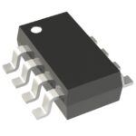 INA190A1QDDFRQ1

The activity of extra discounts on wholesale prices is in full swing…
Please fill in your contact information and we will send you the latest wholesale price list.