ChipApex | Global Electronic Components Supplier

SEARCH
Search Product
Search Post
— IC芯片 | 连接器 | 传感器 | 被动器件 —
Search productSearch post
— IC芯片 | 连接器 | 传感器 | 被动器件 —
Consult the customer manager about the wholesale price.
consultation hotline:86-132-6715-2157
email:[email protected]
Contact the product manager for consultation. One-stop consultation is available.
Do you want a lower wholesale price? Please send us your inquiry and we will reply immediately.
The Texas Instruments INA190A3NDDFREP is a bidirectional, low-power, zero-drift current sense amplifier with an enable pin. It features a fixed gain of 100 V/V and operates from a single supply voltage ranging from 1.7 V to 5.5 V. The device supports common-mode voltages from -0.2 V to +40 V. Key electrical specifications include a maximum offset voltage of ±15 µV, a minimum common-mode rejection ratio of 132 dB, and a typical quiescent current of 50 µA. It is housed in an 8-pin SOT-23-THIN package.
Verify that the specific part number matches the enhanced product (EP) designation required for your application. Confirm that the component meets the necessary defense, aerospace, or medical qualification standards. Ensure the ordering suffix corresponds to the correct tape-and-reel packaging format. Cross-reference the datasheet revision history to confirm the document version aligns with your design requirements.
Select this component when high accuracy and low power consumption are critical. The 100 V/V gain option is suitable for applications requiring moderate signal amplification. Consider the wide common-mode voltage range if sensing is performed on high-side rails. Verify that the operating temperature range of -55°C to +150°C fits the environmental constraints of the target system.
This device belongs to the INA190-EP series, which is designed specifically for rugged environments. It offers controlled baseline manufacturing with extended product life cycles and traceability. The series includes multiple gain options to accommodate various current sensing requirements while maintaining consistent performance characteristics across the family.
Standard commercial variants like the INA190A3IDDFR lack the enhanced product qualifications and extended temperature range. Substituting non-EP versions may compromise reliability in defense or aerospace applications due to differences in fabrication site controls and lifecycle management.
It uses an external voltage applied to the REF pin to offset the output. Positive differential inputs result in an output greater than the reference voltage, while negative inputs result in an output lower than the reference voltage.
The capacitively coupled input blocks DC common-mode voltages from downstream circuits, resulting in very high common-mode rejection ratios and allowing the use of input filters without degrading measurement accuracy.
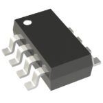 INA190A3NDDFREP

The activity of extra discounts on wholesale prices is in full swing…
Please fill in your contact information and we will send you the latest wholesale price list.