ChipApex | Global Electronic Components Supplier
SEARCH
Search Product
Search Post
— IC芯片 | 连接器 | 传感器 | 被动器件 —
Search productSearch post
— IC芯片 | 连接器 | 传感器 | 被动器件 —
Consult the customer manager about the wholesale price.
consultation hotline:86-132-6715-2157
email:[email protected]
Contact the product manager for consultation. One-stop consultation is available.
Do you want a lower wholesale price? Please send us your inquiry and we will reply immediately.
The INA241B4QDGKRQ1 is an AEC-Q100 qualified, bidirectional current sense amplifier with a fixed gain of 100V/V. It operates over a common-mode voltage range of –5V to 110V and supports supply voltages from 2.7V to 20V. The device features enhanced PWM rejection for switching systems up to 125kHz, high small-signal bandwidth of 1.1MHz, and a slew rate of 8V/µs. It offers a maximum gain error of ±0.1% and offset voltage of ±150µV at 25°C. Available in VSSOP-8 packages, it functions within temperature grades of –40°C to 125°C or 150°C.
Verify the specific suffix QDGKRQ1 corresponds to the VSSOP-8 package and Grade 1 or Grade 0 temperature rating as defined in the TI ordering information. Confirm functional safety documentation requirements if deploying in safety-critical automotive architectures. Ensure input common-mode voltages remain within the specified –5V to 110V operational limits to maintain accuracy and prevent damage.
Select this component when a fixed 100V/V gain is required for high-side, inline, or low-side current sensing applications involving significant common-mode voltage swings. The B-grade variant provides standard precision suitable for general automotive power management. Consider the 1.1MHz bandwidth and PWM rejection capabilities if the application involves noisy switching environments like motor drives or inverters.
This part belongs to the INA241x-Q1 family of ultra-precise, bidirectional current sense amplifiers designed for automotive use. The 'B' designation indicates the B-grade accuracy tier, while '4' specifies the 100V/V gain option. The 'Q1' suffix denotes AEC-Q100 qualification for automotive reliability. Other family members include A-grade variants and different gain options ranging from 10V/V to 200V/V.
Direct substitutes within the same family include INA241A4QDGKRQ1 for higher precision requirements. For different gain configurations, consider INA241B1QDGKRQ1 (10V/V), INA241B2QDGKRQ1 (20V/V), INA241B3QDGKRQ1 (50V/V), or INA241B5QDGKRQ1 (200V/V). All share identical pinouts and core functionality.
It utilizes enhanced PWM rejection circuitry that holds the output for 1μs during large common-mode ΔV/Δt transients, preventing disturbance propagation to the output signal.
The device supports an operational common-mode voltage range from –5V to 110V, which exceeds the power-supply voltage range of 2.7V to 20V.
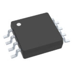 INA241B4QDGKRQ1
The activity of extra discounts on wholesale prices is in full swing…
Please fill in your contact information and we will send you the latest wholesale price list.