 ChipApex | Global Electronic Components Supplier

SEARCH
Search Product
Search Post
— IC芯片 | 连接器 | 传感器 | 被动器件 —
Search productSearch post
— IC芯片 | 连接器 | 传感器 | 被动器件 —
Consult the customer manager about the wholesale price.
consultation hotline:86-132-6715-2157
email:[email protected]
Contact the product manager for consultation. One-stop consultation is available.
Do you want a lower wholesale price? Please send us your inquiry and we will reply immediately.
IP4856CX25/CZ is listed in the Specialized range at ChipApex. The manufacturer field lists Nexperia USA Inc.. Its product description is IC INTFACE SPECIALIZED 25WLCSP. Review the specifications below when checking this part for your BOM.
The IP4856CX25/C is an SD 3.0-compliant 6-bit bidirectional dual voltage level translator designed to interface between memory cards operating at 1.8 V or 2.9 V and hosts with a nominal supply of 1.7 V to 3.6 V. It supports SDR104, SDR50, DDR50, SDR25, SDR12, high-speed (50 MHz), and default-speed (25 MHz) modes. The device features an integrated 100 mA low dropout regulator for card-side I/Os, built-in EMI filters, and robust ESD protection rated at 8 kV contact discharge per IEC 61000-4-2 Level 4. It utilizes a 25-ball WLCSP package with a 0.4 mm pitch.
Verify the specific ordering suffix against the manufacturer's current documentation to ensure correct package configuration and marking codes. Confirm that the component status remains in production before finalizing design-in decisions. Cross-reference the datasheet revision date to ensure all latest electrical characteristics and mechanical dimensions are accounted for in the schematic and layout.
Select this component when interfacing SD memory cards requiring dual voltage translation between host and card domains. Ensure the host supply voltage falls within the 1.7 V to 3.6 V range and the card operates at 1.8 V or 2.9 V. Verify PCB layout capabilities for the 25-ball WLCSP package, specifically regarding micro-via requirements and solder mask apertures for reliable assembly.
This device belongs to Nexperia's portfolio of integrated level translators designed for mobile multimedia applications. It consolidates voltage shifting, regulation, and protection functions into a single compact package, reducing the bill of materials and board space compared to discrete solutions. It is part of the broader family of SD card interface controllers optimized for high-speed data transmission standards.
IP4855CX25
The device includes a feedback channel (CLK_FB) that transmits the clock signal back to the host side. This compensates for propagation delays introduced by the voltage translator and PCB tracks, ensuring accurate timing margins for data read-back from the memory card.
The SEL pin selects the output voltage level of the internal low dropout regulator. A HIGH level configures the regulator for 1.8 V signaling, while a LOW level configures it for 2.9 V signaling, allowing compatibility with different SD card voltage standards.
The device employs a zero-clamping concept where level shifting buffers keep ESD stress away from the host. Any electrostatic discharge on the card-side pins is discharged directly to the supply ground, preventing damage to the host controller.
Explore related parts through Interface, Integrated Circuits (ICs), all product categories, ChipApex homepage.
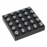 IP4856CX25/CZ

The activity of extra discounts on wholesale prices is in full swing…
Please fill in your contact information and we will send you the latest wholesale price list.






