ChipApex | Global Electronic Components Supplier

SEARCH
Search Product
Search Post
— IC芯片 | 连接器 | 传感器 | 被动器件 —
Search productSearch post
— IC芯片 | 连接器 | 传感器 | 被动器件 —
Consult the customer manager about the wholesale price.
consultation hotline:86-132-6715-2157
email:[email protected]
Contact the product manager for consultation. One-stop consultation is available.
Do you want a lower wholesale price? Please send us your inquiry and we will reply immediately.
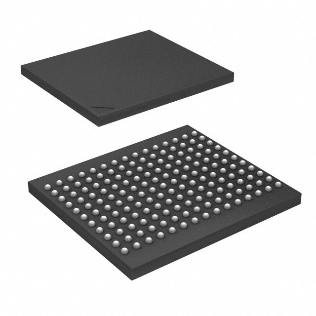
IS61LPS102418A-250B3I is listed in the Memory IC range at ChipApex. The manufacturer field lists ISSI, Integrated Silicon Solution Inc. Its product description is IC SRAM 18MBIT PARALLEL 165TFBGA. Review the specifications below when checking this part for your BOM.
The IS61LPS102418A-250B3I is a high-speed, low-power synchronous static RAM with an 18Mb capacity organized as 1M words by 18 bits. It operates at a clock frequency of 250 MHz with a cycle time of 4 ns and a clock access time of 2.6 ns. The device uses a 165-ball TFBGA package (13x15 mm) and supports Vdd supply voltages from 3.135V to 3.465V. It features pipelined architecture, single-cycle deselect, and individual byte write control.
Verify component authenticity through authorized channels due to potential availability constraints. Confirm that the specific ordering suffix matches the required voltage range and temperature grade. Ensure compliance with RoHS3 standards and check for any product change notices affecting the manufacturing process or specifications before finalizing procurement decisions.
Select this component when a 18Mb synchronous SRAM with 18-bit width is required. Ensure the system design accommodates the 165-TFBGA package dimensions. Verify that the operating environment falls within the specified commercial or industrial temperature ranges. Confirm power supply stability for the 3.3V core and isolated I/O supplies.
This part belongs to the IS61LPS/VPS102418A family of synchronous pipelined SRAMs manufactured by ISSI. It shares architectural similarities with the IS61LPS51236A and IS61LPS25672A variants, differing primarily in organization and package options. The LPS designation indicates a 3.3V core voltage variant.
IS61LPS102418A-250B3LI
The burst sequence order is selected using the MODE pin. Tying the pin LOW achieves a linear burst, while tying it HIGH or leaving it floating results in an interleave burst.
Individual bytes are written using the Byte Write Enable (BWE) input combined with one or more individual byte write signals (BWx). Global Write (GW) can also be used to write all bytes simultaneously.
Explore related parts through Memory, Integrated Circuits (ICs), all product categories, ChipApex homepage.
 IS61LPS102418A-250B3I

The activity of extra discounts on wholesale prices is in full swing…
Please fill in your contact information and we will send you the latest wholesale price list.