 ChipApex | Global Electronic Components Supplier
SEARCH
Search Product
Search Post
— IC芯片 | 连接器 | 传感器 | 被动器件 —
Search productSearch post
— IC芯片 | 连接器 | 传感器 | 被动器件 —
Consult the customer manager about the wholesale price.
consultation hotline:86-132-6715-2157
email:[email protected]
Contact the product manager for consultation. One-stop consultation is available.
Do you want a lower wholesale price? Please send us your inquiry and we will reply immediately.
The ISL21009BFB812Z is a high voltage input precision voltage reference utilizing Intersil's proprietary Floating Gate Analog (FGA) technology. It provides a fixed output voltage of 1.25V with an initial accuracy of ±0.5mV and a temperature coefficient of 3ppm/°C. The device operates within an input voltage range of 3.5V to 16.5V, consuming a maximum supply current of 180µA. It features low output noise of 4.5µV P-P in the 0.1Hz to 10Hz bandwidth and supports an output current capability up to ±7.0mA. The component is housed in an 8-lead SOIC package and functions reliably across an operating temperature range of -40°C to +125°C.
Verify that the specific part number matches the required output voltage, accuracy grade, and temperature coefficient specifications. Confirm the package type and lead configuration align with the PCB footprint requirements. Ensure compliance with RoHS standards and check for any specific handling precautions related to electrostatic discharge during procurement and storage.
Select this component when designing systems requiring high precision voltage references with exceptionally low power consumption. The FGA technology makes it suitable for battery-powered portable instruments where minimizing supply current is critical. Consider the low noise characteristics for applications involving high-resolution data acquisition or sensitive sensor interfaces.
The ISL21009 series belongs to Renesas' (formerly Intersil) FGA™ voltage reference family. This line leverages floating gate CMOS processes to achieve unique stability and low drift characteristics not typically found in standard bandgap references. The ISL21009BFB812Z represents a specific variant within this family optimized for 1.25V output with high initial accuracy.
Direct replacements include other variants within the ISL21009 family such as the ISL21009CFB812Z or ISL21009DFB812Z, which offer different accuracy grades and temperature coefficients while maintaining the same pinout and functionality.
The output voltage can be trimmed up or down by approximately 2.5% using the TRIM pin. This is achieved by connecting a potentiometer between VOUT and GND, with the wiper connected to the TRIM pin.
For load capacitances above 0.001µF, an RC noise reduction network is recommended to maintain stability and improve transient response. Output capacitor values greater than 1.0µF are not recommended without this network.
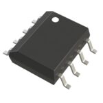 ISL21009BFB812Z
The activity of extra discounts on wholesale prices is in full swing…
Please fill in your contact information and we will send you the latest wholesale price list.





