 ChipApex | Global Electronic Components Supplier

SEARCH
Search Product
Search Post
— IC芯片 | 连接器 | 传感器 | 被动器件 —
Search productSearch post
— IC芯片 | 连接器 | 传感器 | 被动器件 —
Consult the customer manager about the wholesale price.
consultation hotline:86-132-6715-2157
email:[email protected]
Contact the product manager for consultation. One-stop consultation is available.
Do you want a lower wholesale price? Please send us your inquiry and we will reply immediately.
ISPLSI 5256VE-80LF256I is listed in the Complex Programmable Logic Devices range at ChipApex. The manufacturer field lists Lattice Semiconductor Corporation. Its product description is IC CPLD 256MC 12NS 256FPBGA. Review the specifications below when checking this part for your BOM.
The ispLSI 5256VE-80LF256I is a high-density, in-system programmable logic device from Lattice Semiconductor's ispLSI 5000VE family. It features 12,000 PLD gates and 256 macrocells organized into eight Generic Logic Blocks (GLBs). The device utilizes E2CMOS technology with a 3.3V core supply and supports user-selectable 3.3V or 2.5V I/O levels via the VCCIO pin. Key electrical specifications include a maximum operating frequency of 165 MHz and a propagation delay as low as 6.0 ns. It integrates 144 I/O pins, four dedicated clock inputs, and full IEEE 1149.1 boundary scan testability.
Verify that the specific suffix LF256I corresponds to the 256-pin fpBGA package and industrial temperature range (-40°C to +85°C). Confirm that design tools support the ispLSI 5000VE architecture, noting potential differences from the older 5000VA family regarding JEDEC compatibility and feature sets like product term reset logic.
Select this component when designs require 256 registered macrocells and high-speed performance under 3.3V power constraints. Ensure the application benefits from the SuperWIDE GLB structure for complex routing. Verify that the 144 available I/O pins meet system interface requirements and that the BGA package footprint is compatible with the PCB layout.
The ispLSI 5256VE belongs to the second-generation SuperWIDE high-density PLD family. It succeeds earlier ispLSI models by offering enhanced pin-locking capabilities and optimized Generic Logic Blocks. This series is designed for applications demanding high logic density, non-volatile configuration, and robust in-system programmability without the complexity of FPGA architectures.
Direct replacements within the same family include other members of the ispLSI 5000VE series, such as the ispLSI 5128VE, ispLSI 5384VE, or ispLSI 5512VE, depending on macrocell count requirements. Note that the ispLSI 5000VA family is not JEDEC compatible and may have different pinouts or feature availability.
The ispLSI 5000VE is not JEDEC compatible with the 5000VA family. The VE family simplifies Product Term Reset Logic, removes the T-type flip-flop option, and eliminates Global Preset and programmable output-delay features to optimize design fit efficiency.
The device operates on a 3.3V core supply (VCC). Individual I/O pins can be configured for either 3.3V or 2.5V output levels by connecting the VCCIO pin to the desired voltage reference, allowing interoperability with both voltage standards.
Yes, the ispLSI 5256VE supports In-System Programming (ISP) via the IEEE 1149.1-compliant JTAG interface, allowing logic and interconnect structures to be reprogrammed without removing the device from the board.
Explore related parts through Embedded, Integrated Circuits (ICs), all product categories, ChipApex homepage.
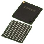 ISPLSI 5256VE-80LF256I

The activity of extra discounts on wholesale prices is in full swing…
Please fill in your contact information and we will send you the latest wholesale price list.






