 ChipApex | Global Electronic Components Supplier

SEARCH
Search Product
Search Post
— IC芯片 | 连接器 | 传感器 | 被动器件 —
Search productSearch post
— IC芯片 | 连接器 | 传感器 | 被动器件 —
Consult the customer manager about the wholesale price.
consultation hotline:86-132-6715-2157
email:[email protected]
Contact the product manager for consultation. One-stop consultation is available.
Do you want a lower wholesale price? Please send us your inquiry and we will reply immediately.
JM38510/30608BEA is listed in the Shift Registers range at ChipApex. The manufacturer field lists Texas Instruments. Its product description is PARALLEL-LOAD 8-BIT SHIFT REGIST. Review the specifications below when checking this part for your BOM.
The Texas Instruments JM38510/30608BEA is a military-grade parallel-load 8-bit shift register belonging to the SN54LS165A family. It features eight direct data inputs and serial output capabilities within a 16-pin ceramic dual in-line package (CDIP). The device operates across an extended temperature range of -55°C to 125°C, utilizing LS logic standards for low power consumption. Key functional inputs include a gated clock, clock inhibit, and a shift/load control pin that enables immediate parallel data loading.
Verify the specific ordering suffix against current TI documentation, as status classifications such as NRND may apply to certain variants. Confirm compliance with MIL-PRF-38535 requirements if full parameter testing is mandated for the application environment.
Select this component when a robust, radiation-tolerant shift register is required for harsh environments. Ensure the design accommodates the 16-pin CDIP footprint and utilizes the LS logic voltage levels. Verify that the clock frequency requirements align with the specified maximum operating limits for the LS series.
This part number represents a QML-certified version of the SN54LS165A, designed for military and defense applications. It falls under the broader SN54/74LS165A family of parallel-load shift registers, offering enhanced reliability compared to standard commercial equivalents.
Public confirmed substitute part numbers: JM38510/30608B2A, JM38510/30608BFA, M38510/30608B2A, M38510/30608BFA.
Parallel data is loaded directly into the register when the shift/load (SH/LD) input is held at a low level, independent of the clock or serial input states.
The CLK INH input serves as a clock-inhibit function; holding it high inhibits clocking regardless of the state of the primary clock input.
Explore related parts through Logic, Integrated Circuits (ICs), all product categories, ChipApex homepage.
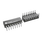 JM38510/30608BEA

The activity of extra discounts on wholesale prices is in full swing…
Please fill in your contact information and we will send you the latest wholesale price list.





