ChipApex | Global Electronic Components Supplier

SEARCH
Search Product
Search Post
— IC芯片 | 连接器 | 传感器 | 被动器件 —
Search productSearch post
— IC芯片 | 连接器 | 传感器 | 被动器件 —
Consult the customer manager about the wholesale price.
consultation hotline:86-132-6715-2157
email:[email protected]
Contact the product manager for consultation. One-stop consultation is available.
Do you want a lower wholesale price? Please send us your inquiry and we will reply immediately.
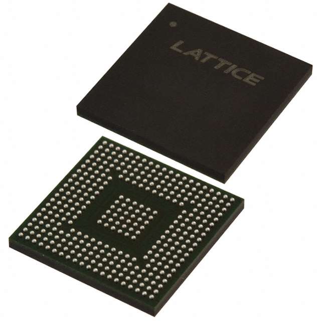
LCMXO2-4000HC-4BG332C is listed in the Field Programmable Gate Array range at ChipApex. The manufacturer field lists Lattice Semiconductor Corporation. Its product description is IC FPGA 274 I/O 332CABGA. Review the specifications below when checking this part for your BOM.
The LCMXO2-4000HC-4BG332C is a Field Programmable Gate Array (FPGA) from the Lattice MachXO2 family, manufactured by Lattice Semiconductor. It features 4320 Logic Elements (LEs), organized as 2160 Adaptive Logic Modules (ALMs) and 540 Logic Array Blocks (LABs). The device includes 92 kbit of embedded block RAM and 34 kbit of distributed RAM, totaling 222 kbit of memory resources. It provides 274 I/O pins and operates within a supply voltage range of 2.375 V to 3.6 V, with typical operation at 2.5 V or 3.3 V. The maximum operating frequency is 269 MHz. It supports an industrial temperature range of 0°C to +85°C and is housed in a CABGA-332 package.
Verify the specific suffix 'C' indicates commercial temperature range (0°C to +85°C) against the official datasheet. Confirm the CABGA-332 package dimensions and pinout compatibility with the target PCB footprint. Ensure the design tool version supports the MachXO2 architecture for bitstream generation.
Select this model when 4320 LEs and 274 I/Os are required in a compact BGA form factor. Compare against the BG256 variant if fewer pins suffice. Verify that the 269 MHz speed grade meets timing requirements. Consider the HC variant characteristics for high-performance logic density within the MachXO2 series.
This component belongs to the Lattice MachXO2 series, designed for low-power, cost-sensitive FPGA applications. It serves as a drop-in replacement for complex PLDs and GALs. The MachXO2 family emphasizes ease of use and rapid prototyping capabilities for small to medium-scale logic designs.
Direct substitutes include other LCMXO2-4000 variants with different packages such as LCMXO2-4000HC-4BG256I or LCMXO2-4000HC-4FG484I, provided pin counts and thermal requirements align. Cross-family replacements require careful review of logic capacity and I/O configurations.
Explore related parts through Embedded, Integrated Circuits (ICs), all product categories, ChipApex homepage.


 LCMXO2-4000HC-4BG332C

The activity of extra discounts on wholesale prices is in full swing…
Please fill in your contact information and we will send you the latest wholesale price list.