ChipApex | Global Electronic Components Supplier
SEARCH
Search Product
Search Post
— IC芯片 | 连接器 | 传感器 | 被动器件 —
Search productSearch post
— IC芯片 | 连接器 | 传感器 | 被动器件 —
Consult the customer manager about the wholesale price.
consultation hotline:86-132-6715-2157
email:[email protected]
Contact the product manager for consultation. One-stop consultation is available.
Do you want a lower wholesale price? Please send us your inquiry and we will reply immediately.
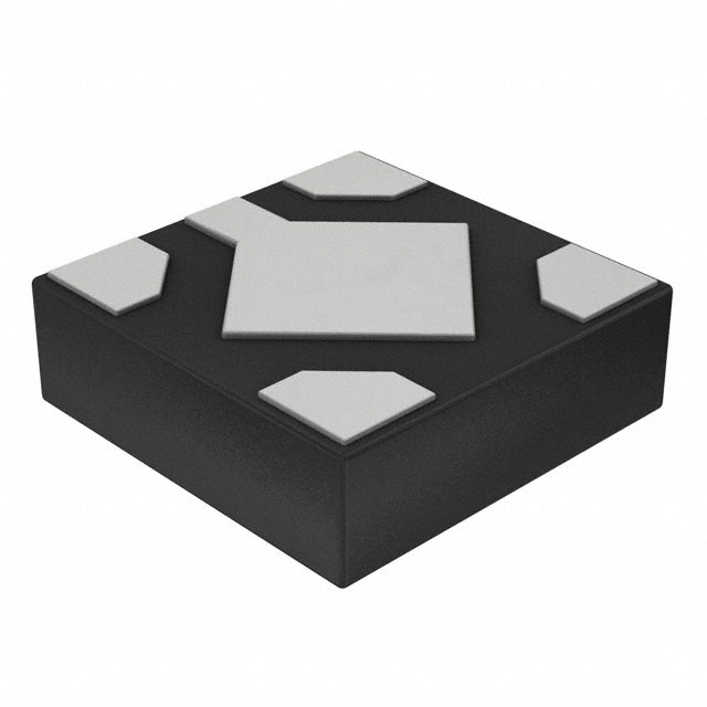
The LD56050DPU115R is a high-accuracy linear regulator providing a fixed 1.15 V output with a guaranteed 500 mA current capability. It utilizes an NMOS pass transistor biased by a dedicated pin to achieve ultra-low dropout performance, even at low input voltages. The device operates within an input voltage range of 0.8 V to 5.5 V and features a low ground current of 27 μA typical at no-load. Output voltage tolerance is ±0.5% at 25 °C and ±1.5% over the full temperature range. It includes logic-controlled shutdown consuming less than 0.1 µA, internal current limiting with foldback, thermal shutdown, and an active output discharge function.
Verify the specific ordering suffix DPU115R corresponds to the required 1.15 V fixed output voltage and the presence of the output discharge function. Confirm that the DFN4 1.2 x 1.2 mm package dimensions align with the target PCB footprint requirements. Ensure the application design accounts for the external ceramic capacitor specifications necessary for loop stability across the operating temperature range.
Select this component when space-constrained designs require a compact DFN4 1.2 x 1.2 mm package. It is suitable for battery-operated applications due to its low quiescent current and efficient shutdown mode. Designers must ensure the bias supply voltage meets the minimum requirement relative to the output voltage to maintain regulation. Verify that the load transient response requirements are met by the specified output capacitance range.
The LD56050DPU115R belongs to the LD56050 family of ultra-low dropout linear regulators manufactured by STMicroelectronics. This series is characterized by high accuracy and low power consumption, specifically engineered for portable electronics. The DPU115R variant specifies the fixed 1.15 V output voltage option within the product line, distinguishing it from other voltage configurations available in the same package.
LD56050DPU110R
The device integrates an output discharge MOSFET that activates when the EN pin goes to a low logic level, quickly discharging the output capacitor.
The VBIAS pin supplies the internal driving and control circuitry. It requires a minimum voltage typically 1.6 V higher than the output to properly bias the N-channel power element.
 LD56050DPU115R
The activity of extra discounts on wholesale prices is in full swing…
Please fill in your contact information and we will send you the latest wholesale price list.