ChipApex | Global Electronic Components Supplier
SEARCH
Search Product
Search Post
— IC芯片 | 连接器 | 传感器 | 被动器件 —
Search productSearch post
— IC芯片 | 连接器 | 传感器 | 被动器件 —
Consult the customer manager about the wholesale price.
consultation hotline:86-132-6715-2157
email:[email protected]
Contact the product manager for consultation. One-stop consultation is available.
Do you want a lower wholesale price? Please send us your inquiry and we will reply immediately.
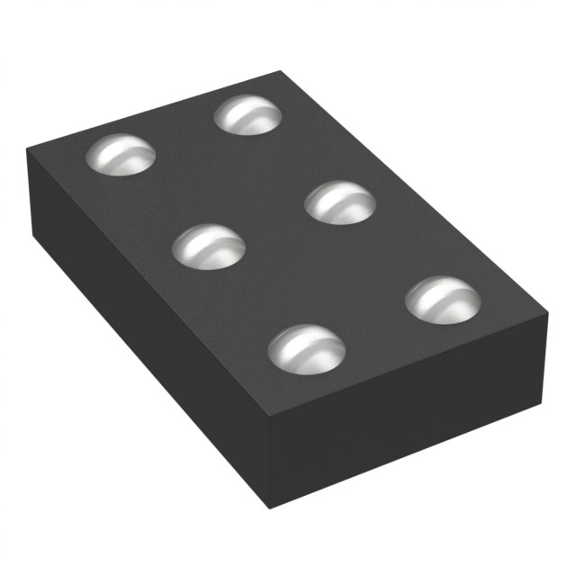
The LD57100J100R is a fixed-output low-dropout linear regulator providing 1.0 V at up to 1 A. It utilizes an NMOS pass transistor with a dedicated bias pin (VBIAS) for ultra-low dropout performance, typically 40 mV at full load. The input voltage range extends from the output voltage to 5.5 V, while the bias supply requires 3.0 V to 5.5 V. Quiescent current is 35 µA typical. The device features logic-controlled shutdown consuming less than 0.1 µA, internal current limiting, and thermal protection. It is housed in a Flip Chip6 package measuring 0.8 x 1.2 mm.
Verify the specific ordering code LD57100J100R against the manufacturer's datasheet to confirm the 1.0 V fixed output voltage and Flip Chip6 packaging. Ensure the design accounts for the required VBIAS pin voltage constraints, which must be between 3.0 V and 5.5 V or at least 1.6 V above the output voltage. Confirm that the application environment operates within the specified -40 °C to +85 °C temperature range for guaranteed electrical characteristics.
Select this component when space-constrained designs require a high-current LDO with minimal voltage headroom. The dedicated bias pin allows operation even when the main input voltage is very close to the output level. Consider the Flip Chip6 package dimensions for PCB layout optimization. Ensure the application can provide the necessary bias voltage to the VBIAS pin to maintain the ultra-low dropout performance specified in the datasheet.
The LD57100 series belongs to STMicroelectronics' portfolio of high-accuracy voltage regulators designed for battery-operated applications. This specific part is a fixed-output variant within the family, distinguished by its 1.0 V nominal output. The series emphasizes space efficiency through its compact Flip Chip6 footprint and low quiescent current consumption, targeting portable electronics where power management and physical size are critical constraints.
Consult the official STMicroelectronics datasheet for verified substitute part numbers within the LD57100 series or other compatible LDO families. Do not assume functional equivalence based on generic specifications; verify pin compatibility, electrical parameters, and package dimensions against the source documentation before substitution.
The VBIAS pin supplies the internal control circuitry and biases the gate of the NMOS pass transistor. Maintaining the VBIAS voltage at least 1.6 V above the output voltage (minimum 3.0 V) ensures the transistor remains fully enhanced, enabling the ultra-low dropout performance even at very low input voltages.
In the fixed output version, such as the LD57100J100R, the SNS/FB pin serves as the Output Voltage Sense pin. It should be connected to the load using a separate PCB track to compensate for voltage drops across the board traces, ensuring accurate regulation at the load point.
 LD57100J100R
The activity of extra discounts on wholesale prices is in full swing…
Please fill in your contact information and we will send you the latest wholesale price list.