ChipApex | Global Electronic Components Supplier
SEARCH
Search Product
Search Post
— IC芯片 | 连接器 | 传感器 | 被动器件 —
Search productSearch post
— IC芯片 | 连接器 | 传感器 | 被动器件 —
Consult the customer manager about the wholesale price.
consultation hotline:86-132-6715-2157
email:[email protected]
Contact the product manager for consultation. One-stop consultation is available.
Do you want a lower wholesale price? Please send us your inquiry and we will reply immediately.
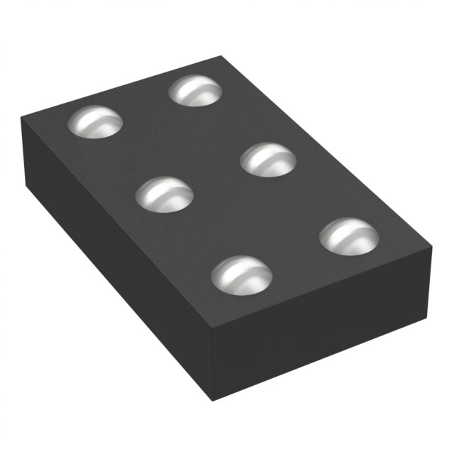
The LD57100J105R is a fixed-output ultra low-dropout linear regulator from STMicroelectronics, providing a nominal output voltage of 1.05 V with a guaranteed maximum load current of 1 A. It operates within an input voltage range extending from the output level up to 5.5 V and requires a dedicated bias supply between 3.0 V and 5.5 V. The device features a typical dropout voltage of 40 mV at full load and maintains an output accuracy of ±0.5% at 25 °C. Packaged in a Flip Chip6 (0.8x1.2 mm) format, it supports operation across a temperature range of -40 °C to +85 °C.
Verify the specific ordering code LD57100J105R against the manufacturer's official datasheet DS13123 Rev 6 to confirm the 1.05 V fixed output specification. Ensure the design accommodates the required external ceramic capacitors and the separate VBIAS supply rail as detailed in the application circuits section.
Select this component when space-constrained designs require a high-current LDO with minimal footprint. The Flip Chip6 package maximizes board area efficiency. Designers must ensure the bias pin receives a minimum of 3.0 V or VOUT plus 1.6 V to maintain proper regulation and low dropout characteristics under all operating conditions.
This part belongs to the LD57100 series of 1 A ultra low-dropout regulators. The series offers various fixed output voltages ranging from 0.8 V to 3.3 V, alongside adjustable versions. All variants share the same compact Flip Chip6 packaging and core protection features, differing primarily in their internal reference settings and output tolerance specifications.
Other members of the LD57100 family provide identical functionality with different fixed output voltages, such as LD57100J100R (1.00 V), LD57100J110R (1.10 V), and LD57100J120R (1.20 V). These parts are pin-compatible and suitable for direct substitution if the system power rail requirements allow for the alternative voltage levels.
The VBIAS pin supplies the internal driving circuitry. To achieve the specified ultra-low dropout, the bias voltage must be maintained at a minimum of 3.0 V or VOUT plus 1.6 V, whichever is greater.
When the Enable pin is driven low, the device enters shutdown mode with current consumption below 0.1 µA. Simultaneously, an internal MOSFET activates to actively discharge the output capacitor.
 LD57100J105R
The activity of extra discounts on wholesale prices is in full swing…
Please fill in your contact information and we will send you the latest wholesale price list.