ChipApex | Global Electronic Components Supplier
SEARCH
Search Product
Search Post
— IC芯片 | 连接器 | 传感器 | 被动器件 —
Search productSearch post
— IC芯片 | 连接器 | 传感器 | 被动器件 —
Consult the customer manager about the wholesale price.
consultation hotline:86-132-6715-2157
email:[email protected]
Contact the product manager for consultation. One-stop consultation is available.
Do you want a lower wholesale price? Please send us your inquiry and we will reply immediately.
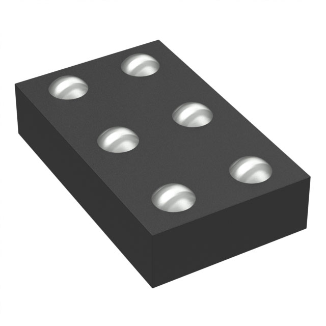
The LD57100J330R is a fixed-output low-dropout linear regulator from STMicroelectronics, providing a nominal output voltage of 3.3 V with a guaranteed maximum load current of 1 A. It utilizes an NMOS pass transistor biased by a dedicated pin to achieve ultra-low dropout performance, typically 40 mV at full load. The device operates with an input voltage range extending from the output voltage up to 5.5 V and requires a separate bias supply between 3.0 V and 5.5 V. It features high accuracy with ±1% output voltage tolerance over the temperature range and includes logic-controlled shutdown for ultra-low standby consumption.
Verify the specific ordering code LD57100J330R against the manufacturer's official datasheet DS13123 Rev 6 to confirm the 3.3 V fixed output specification. Ensure compatibility with the required Flip Chip6 (0.8x1.2 mm) package footprint during PCB layout. Confirm that the application circuit provides the necessary external ceramic capacitors and bias voltage conditions as defined in the recommended operating parameters.
Select this component for battery-operated applications requiring high efficiency at low input-to-output differentials. The dedicated bias pin allows the use of lower input voltages compared to standard LDOs, provided the bias rail meets the minimum 3.0 V requirement. Designers must account for the specific thermal resistance and ensure adequate heat dissipation within the compact Flip Chip6 package to maintain junction temperatures within the specified operating range.
The LD57100 series belongs to STMicroelectronics' portfolio of power management integrated circuits, specifically designed as ultra-low-dropout regulators. This family emphasizes space-saving packaging and low quiescent current to extend battery life in portable electronics. The J330 suffix identifies the specific variant within the series configured for a fixed 3.3 V output, distinguishing it from adjustable or other fixed voltage options.
LD57100J330R
The device integrates a MOSFET between VOUT and GND that activates when the EN pin goes low, quickly discharging the output capacitor upon shutdown.
The VBIAS pin supplies the internal driving and control circuitry, allowing the NMOS pass transistor gate to be properly biased for ultra-low dropout performance even at low input voltages.
 LD57100J330R
The activity of extra discounts on wholesale prices is in full swing…
Please fill in your contact information and we will send you the latest wholesale price list.