 ChipApex | Global Electronic Components Supplier
SEARCH
Search Product
Search Post
— IC芯片 | 连接器 | 传感器 | 被动器件 —
Search productSearch post
— IC芯片 | 连接器 | 传感器 | 被动器件 —
Consult the customer manager about the wholesale price.
consultation hotline:86-132-6715-2157
email:[email protected]
Contact the product manager for consultation. One-stop consultation is available.
Do you want a lower wholesale price? Please send us your inquiry and we will reply immediately.
The LD6806F/14P,115 is a low-dropout regulator (LDO) from the NXP LD6806 series, featuring a fixed 1.4 V output voltage and a 200 mA current rating. It operates within an input voltage range of 2.3 V to 5.5 V and delivers a typical dropout voltage of 60 mV at full load. The device incorporates a pull-down switching transistor for a low-ohmic output state when disabled. Key electrical characteristics include a typical quiescent current of 70 µA, 30 µV RMS output noise, and 55 dB power supply rejection ratio at 1 kHz. It provides integrated thermal protection, current limiting, and 10 kV Human Body Model ESD protection.
Verify the specific ordering suffix ',115' against official NXP documentation to confirm tape-and-reel packaging specifications. Ensure the selected package variant matches the required PCB footprint dimensions for the SOT886 (XSON6) outline. Confirm that the fixed 1.4 V output aligns with the target circuit design requirements before procurement.
Select this component for applications demanding precise 1.4 V regulation with minimal voltage drop under heavy loads. The LD6806F/14P is suitable where low quiescent current and fast transient response are critical. Consider the SOT886 package size constraints and verify that external capacitors meet the minimum 0.7 µF capacitance requirement for stability across the operating temperature range.
The LD6806 series comprises ultra-low-dropout regulators designed for space-constrained portable electronics. Available in WLCSP4, SOT886, and SOT753 packages, the family offers various fixed output voltages ranging from 1.2 V to 3.6 V. The 'H' variants feature a high-ohmic output state when disabled, whereas 'P' variants utilize a pull-down transistor for rapid discharge, catering to different system power management strategies.
Direct replacements must match the 1.4 V fixed output, 200 mA rating, and SOT886 package. Verify compatibility with other LD6806 series members if output voltage flexibility is acceptable. Cross-reference pinouts and thermal resistance values to ensure equivalent performance in the existing layout without redesigning the power stage.
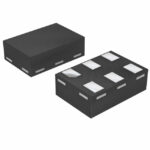 LD6806F/14P,115
The activity of extra discounts on wholesale prices is in full swing…
Please fill in your contact information and we will send you the latest wholesale price list.




