 ChipApex | Global Electronic Components Supplier

SEARCH
Search Product
Search Post
— IC芯片 | 连接器 | 传感器 | 被动器件 —
Search productSearch post
— IC芯片 | 连接器 | 传感器 | 被动器件 —
Consult the customer manager about the wholesale price.
consultation hotline:86-132-6715-2157
email:[email protected]
Contact the product manager for consultation. One-stop consultation is available.
Do you want a lower wholesale price? Please send us your inquiry and we will reply immediately.
LFE2-12SE-7F256C is listed in the Field Programmable Gate Array range at ChipApex. The manufacturer field lists Lattice Semiconductor Corporation. Its product description is IC FPGA 193 I/O 256FBGA. Review the specifications below when checking this part for your BOM.
The LFE2-12SE-7F256C is a Field Programmable Gate Array (FPGA) from the Lattice ECP2M family, manufactured by Lattice Semiconductor Corporation. It features 6000 Adaptive Logic Modules (ALMs), equivalent to 12000 logic elements, and provides 148 I/O pins. The device includes 936 kbit of embedded block RAM and 24 kbit of distributed RAM, totaling approximately 960 kbit of memory resources. It operates with a core voltage range of 1.14 V to 1.26 V and supports data rates up to 622 Mb/s via its SERDES interface. The component is housed in a 256-ball Fine-Pitch Ball Grid Array (FPBGA) package, measuring 17x17 mm, and is rated for commercial operating temperatures between 0°C and +85°C.
Verify the specific speed grade suffix '7' corresponds to the required timing performance for your design constraints. Confirm the package type FPBGA-256 matches your PCB footprint requirements. Check RoHS compliance status if environmental regulations apply to your manufacturing process. Ensure availability of compatible programming tools such as Lattice Diamond or Radiant software for configuration.
Select this model when designs require moderate logic density around 12k LEs with integrated high-speed serial capabilities. Compare against other ECP2M variants if higher I/O counts or larger memory resources are needed. Consider the thermal characteristics of the FPBGA package for heat dissipation in enclosed enclosures. Evaluate power consumption estimates against system battery or supply limitations.
This component belongs to the Lattice ECP2M series, which focuses on low-power FPGA solutions with embedded DSP and SERDES capabilities. It serves as an intermediate-density option within the Lattice portfolio, bridging the gap between smaller MachXO devices and larger ECP5 families. The series is known for balancing cost, power, and performance for connectivity and control applications.
Direct pin-to-pin replacements may not exist due to unique architectural differences. Review Lattice's official cross-reference guides for functional equivalents within the ECP2M or ECP5 families. Verify that alternative devices support the same SERDES speeds and I/O standards required by the original design specifications.
Explore related parts through Embedded, Integrated Circuits (ICs), all product categories, ChipApex homepage.


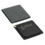 LFE2-12SE-7F256C

The activity of extra discounts on wholesale prices is in full swing…
Please fill in your contact information and we will send you the latest wholesale price list.




