 ChipApex | Global Electronic Components Supplier

SEARCH
Search Product
Search Post
— IC芯片 | 连接器 | 传感器 | 被动器件 —
Search productSearch post
— IC芯片 | 连接器 | 传感器 | 被动器件 —
Consult the customer manager about the wholesale price.
consultation hotline:86-132-6715-2157
email:[email protected]
Contact the product manager for consultation. One-stop consultation is available.
Do you want a lower wholesale price? Please send us your inquiry and we will reply immediately.
LFE2-35SE-5F672I is listed in the Field Programmable Gate Array range at ChipApex. The manufacturer field lists Lattice Semiconductor Corporation. Its product description is IC FPGA 450 I/O 672FPBGA. Review the specifications below when checking this part for your BOM.
The LFE2-35SE-5F672I is a Field Programmable Gate Array (FPGA) from the Lattice ECP2M family, manufactured by Lattice Semiconductor Corporation. It features 34,000 logic elements and 17,000 Adaptive Logic Modules (ALMs). The device includes 2.05 Mbit of embedded memory, comprising 71 kbit distributed RAM and 2,101 kbit Embedded Block RAM (EBR). It supports up to 410 I/Os and operates at a maximum frequency of 320 MHz with data rates up to 750 Mb/s. Power supply voltage ranges from 1.14 V to 1.26 V. Operating temperature spans -40°C to +100°C. The component is housed in a 672-pin FPBGA package.
Verify component authenticity through authorized distributors or direct manufacturer channels. Confirm RoHS compliance status as indicated in official documentation. Check for end-of-life notices or obsolescence warnings prior to procurement. Ensure packaging integrity matches specified SMD/SMT requirements. Validate part number suffixes against current Lattice Semiconductor catalogs.
Compare logic density and I/O count against project requirements. Evaluate power consumption profiles relative to available thermal management solutions. Assess compatibility with existing design tools such as Lattice Diamond. Consider package availability and lead times for production scaling. Review pinout configurations for interface alignment with target peripherals.
This FPGA belongs to the Lattice ECP2M series, designed for mid-range performance applications requiring low power consumption. The series integrates hard macro blocks for DSP and memory functions. It targets markets needing flexible logic reconfiguration with minimal energy usage. The FPBGA-672 package provides high I/O density for complex system integration.
LFE2M35E-5F672I: Pin-compatible upgrade within the same family offering enhanced speed grades. LFE2M35SE-6F672I: Higher speed grade variant with identical pinout and logical structure. Verify software toolchain support for any selected replacement before implementation.
Explore related parts through Embedded, Integrated Circuits (ICs), all product categories, ChipApex homepage.
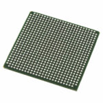 LFE2-35SE-5F672I

The activity of extra discounts on wholesale prices is in full swing…
Please fill in your contact information and we will send you the latest wholesale price list.






