ChipApex | Global Electronic Components Supplier

SEARCH
Search Product
Search Post
— IC芯片 | 连接器 | 传感器 | 被动器件 —
Search productSearch post
— IC芯片 | 连接器 | 传感器 | 被动器件 —
Consult the customer manager about the wholesale price.
consultation hotline:86-132-6715-2157
email:[email protected]
Contact the product manager for consultation. One-stop consultation is available.
Do you want a lower wholesale price? Please send us your inquiry and we will reply immediately.
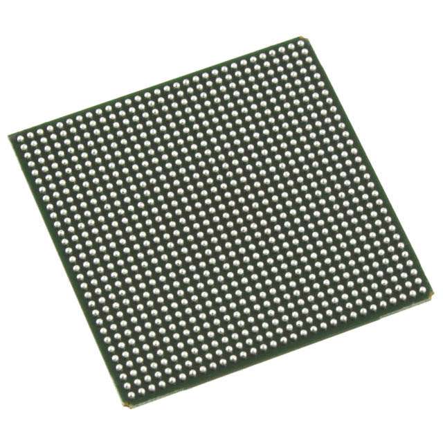
LFE2M100E-5F900I is listed in the Field Programmable Gate Array range at ChipApex. The manufacturer field lists Lattice Semiconductor Corporation. Its product description is IC FPGA 416 I/O 900FBGA. Review the specifications below when checking this part for your BOM.
The LFE2M100E-5F900I is a Field Programmable Gate Array from the Lattice ECP2M family, manufactured by Lattice Semiconductor Corporation. It features 95,000 logic elements and 11,875 Logic Array Blocks (LABs). The device integrates 5,435,392 bits of total embedded memory, comprising Embedded Block RAM and Distributed RAM. It supports up to 520 I/O pins and operates within a supply voltage range of 1.14 V to 1.26 V. The component is rated for industrial temperatures between -40°C and +100°C TJ and utilizes a 1152-ball FPBGA package.
Verify the specific suffix against official documentation, as variations may indicate differences in temperature grades or packaging. Confirm current availability status directly with authorized distributors, as lead times can vary significantly. Ensure compliance with RoHS directives and moisture sensitivity levels prior to assembly planning.
Select this model when designs require significant logic density combined with embedded memory resources. The ECP2M architecture is suitable for applications needing flexible I/O standards and moderate speed performance. Evaluate thermal requirements carefully given the operating junction temperature range and power consumption characteristics typical of this FPGA family.
This component belongs to the Lattice ECP2M series, which bridges the gap between low-end CPLDs and high-end FPGAs. The series is characterized by its non-volatile configuration memory and low static power consumption. It targets cost-sensitive applications that still demand substantial programmability and connectivity options.
LFE2M100E-5FN1152I is a confirmed substitute part number offering identical functional specifications and pinout compatibility within the same product family.
Explore related parts through Embedded, Integrated Circuits (ICs), all product categories, ChipApex homepage.


 LFE2M100E-5F900I

The activity of extra discounts on wholesale prices is in full swing…
Please fill in your contact information and we will send you the latest wholesale price list.