 ChipApex | Global Electronic Components Supplier

SEARCH
Search Product
Search Post
— IC芯片 | 连接器 | 传感器 | 被动器件 —
Search productSearch post
— IC芯片 | 连接器 | 传感器 | 被动器件 —
Consult the customer manager about the wholesale price.
consultation hotline:86-132-6715-2157
email:[email protected]
Contact the product manager for consultation. One-stop consultation is available.
Do you want a lower wholesale price? Please send us your inquiry and we will reply immediately.
LFEC3E-3T100I is listed in the Field Programmable Gate Array range at ChipApex. The manufacturer field lists Lattice Semiconductor Corporation. Its product description is IC FPGA 67 I/O 100TQFP. Review the specifications below when checking this part for your BOM.
The LFEC3E-3T100I is a Field Programmable Gate Array (FPGA) from the LatticeECP/EC family, manufactured by Lattice Semiconductor Corporation. It features 3100 logic elements and 67 I/Os in a 100-LQFP package. The device operates at a minimum voltage of 1.14 V and maximum of 1.26 V, with a standard working voltage of 1.2 V. It includes 56320 bits of total RAM, comprising distributed and embedded block memory. The component supports surface mount installation and functions within a temperature range of -40°C to +100°C.
This component is listed as obsolete or discontinued by the manufacturer. Availability is restricted, and sourcing may require checking secondary market distributors. Verify end-of-life status and lead times carefully before integration into new designs. Ensure compatibility with existing supply chain channels for legacy parts.
Select this FPGA for applications requiring moderate logic density and low power consumption. The 1.2V core voltage supports energy-efficient designs. Consider the 100-pin package size for space-constrained PCB layouts. Evaluate the 67 I/O count against interface requirements to ensure sufficient connectivity without excessive pin allocation.
Part of the LatticeECP/EC family, designed for cost-effective and power-efficient programmable logic solutions. The series targets industrial, telecom, and automotive markets, emphasizing reliability and low power usage. This specific model represents an older generation within the Lattice portfolio, preceding newer high-performance families.
No direct public substitute part numbers are confirmed for this obsolete component. Designers should evaluate newer Lattice ECP5 or CrossLink-N families for functional equivalents, considering differences in logic capacity, I/O counts, and package dimensions during migration.
Explore related parts through Embedded, Integrated Circuits (ICs), all product categories, ChipApex homepage.
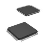 LFEC3E-3T100I

The activity of extra discounts on wholesale prices is in full swing…
Please fill in your contact information and we will send you the latest wholesale price list.






