 ChipApex | Global Electronic Components Supplier

SEARCH
Search Product
Search Post
— IC芯片 | 连接器 | 传感器 | 被动器件 —
Search productSearch post
— IC芯片 | 连接器 | 传感器 | 被动器件 —
Consult the customer manager about the wholesale price.
consultation hotline:86-132-6715-2157
email:[email protected]
Contact the product manager for consultation. One-stop consultation is available.
Do you want a lower wholesale price? Please send us your inquiry and we will reply immediately.
LFXP15C-3F484C is listed in the Field Programmable Gate Array range at ChipApex. The manufacturer field lists Lattice Semiconductor Corporation. Its product description is IC FPGA 300 I/O 484FBGA. Review the specifications below when checking this part for your BOM.
The LFXP15C-3F484C is a Field Programmable Gate Array from the LatticeXP family, featuring 15.4K logic cells (LUTs) and 324 Kbits of Embedded Block RAM. It operates at speed grade -3 within a 484-pin fpBGA package measuring 23x23 mm. The device supports core voltages of 1.2V, 1.8V, 2.5V, or 3.3V and includes four sysCLOCK PLLs for clock management.
Verify the specific ordering suffix against the manufacturer's official documentation to confirm voltage options and temperature grades. Ensure compatibility with the ispLEVER design tool suite for implementation. Confirm package dimensions match the target PCB footprint requirements before finalizing procurement.
Select this component when non-volatile storage and instant-on functionality are required to eliminate external configuration flash. Consider the 15.4K LUT density and 324 Kbit EBR capacity for moderate complexity designs. Evaluate the 484-ball BGA package constraints for routing and thermal management during the initial hardware design phase.
This device belongs to the LatticeXP family, which utilizes next-generation ispXP technology. This architecture integrates logic gates, embedded memory, and high-performance I/Os into a single non-volatile chip. The family is designed to support cost-effective system designs by removing the need for expensive external configuration memories.
Devices within the same LatticeXP family offer density migration options. Verify pin-to-pin compatibility and electrical specifications when considering alternative part numbers from the LFXP series.
Explore related parts through Embedded, Integrated Circuits (ICs), all product categories, ChipApex homepage.


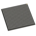 LFXP15C-3F484C

The activity of extra discounts on wholesale prices is in full swing…
Please fill in your contact information and we will send you the latest wholesale price list.




