ChipApex | Global Electronic Components Supplier

SEARCH
Search Product
Search Post
— IC芯片 | 连接器 | 传感器 | 被动器件 —
Search productSearch post
— IC芯片 | 连接器 | 传感器 | 被动器件 —
Consult the customer manager about the wholesale price.
consultation hotline:86-132-6715-2157
email:[email protected]
Contact the product manager for consultation. One-stop consultation is available.
Do you want a lower wholesale price? Please send us your inquiry and we will reply immediately.
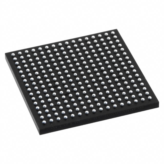
LFXP2-30E-7FT256C is listed in the Field Programmable Gate Array range at ChipApex. The manufacturer field lists Lattice Semiconductor Corporation. Its product description is IC FPGA 201 I/O 256FTBGA. Review the specifications below when checking this part for your BOM.
The LFXP2-30E-7FT256C is a Field Programmable Gate Array from the LatticeXP2 family, manufactured by Lattice Semiconductor. It features approximately 30K logic elements and 14,500 Adaptive Logic Modules within an FTBGA-256 package. The device includes 387 kbit of embedded block RAM and 56 kbit of distributed RAM, totaling 443 kbit of memory resources. It supports up to 201 I/Os and operates at a maximum frequency of 420 MHz with a core voltage range of 1.14 V to 1.26 V. Designed for industrial temperature ranges (0°C to +85°C), this component integrates Flash-based non-volatile configuration architecture.
Verify component authenticity as the LFXP2-30E-7FT256C is listed as obsolete or end-of-life by the manufacturer. Confirm RoHS compliance status, as some sources indicate non-compliance for specific manufacturing dates. Ensure proper handling for moisture sensitivity level 3 devices and validate lead integrity before soldering.
Select this model when instant-on capability and low system cost are required without external configuration flash. Consider the 256-pin FTBGA package constraints and verify that the 30K LUT capacity meets logic density requirements. Check if the 1.2V core voltage aligns with available power rails in the target design environment.
This part belongs to the LatticeXP2 series, which utilizes a third-generation non-volatile FPGA architecture. The series is optimized for high-volume, low-cost applications requiring small footprints and on-chip storage. It sits between the older LatticeXP and the higher-performance LatticeECP3 families in terms of feature set and density.
Publicly confirmed substitute part numbers are not available in the provided documentation. As the device is marked as obsolete, alternative solutions may require redesigning the PCB footprint or utilizing compatible devices from the same LatticeXP2 family with different pin counts or densities.
Explore related parts through Embedded, Integrated Circuits (ICs), all product categories, ChipApex homepage.
 LFXP2-30E-7FT256C

The activity of extra discounts on wholesale prices is in full swing…
Please fill in your contact information and we will send you the latest wholesale price list.