 ChipApex | Global Electronic Components Supplier

SEARCH
Search Product
Search Post
— IC芯片 | 连接器 | 传感器 | 被动器件 —
Search productSearch post
— IC芯片 | 连接器 | 传感器 | 被动器件 —
Consult the customer manager about the wholesale price.
consultation hotline:86-132-6715-2157
email:[email protected]
Contact the product manager for consultation. One-stop consultation is available.
Do you want a lower wholesale price? Please send us your inquiry and we will reply immediately.
LMK1D1204PRHDT is listed in the Clock Buffers, Drivers range at ChipApex. The manufacturer field lists Texas Instruments. Its product description is IC CLK BUFFER 2:4 2GHZ 28VQFN. Review the specifications below when checking this part for your BOM.
The LMK1D1204PRHDT is a low additive jitter LVDS clock buffer manufactured by Texas Instruments. It features a 2:4 architecture, distributing one of two selectable inputs (IN0 or IN1) to four differential LVDS outputs. The device supports input frequencies up to 2 GHz and operates with supply voltages of 1.8 V, 2.5 V, or 3.3 V ± 5%. Key electrical specifications include a maximum propagation delay of 575 ps, output skew of 20 ps, and additive jitter less than 60 fs RMS at 156.25 MHz. It is housed in a 28-pin VQFN package.
Verify the ordering suffix 'RHDT' corresponds to the specific tape-and-reel packaging configuration required for the assembly process. Confirm that the component meets RoHS compliance standards as specified in the manufacturer's documentation. Ensure the procurement source provides valid traceability for the production lot.
Select this component when individual output control is required, distinguishing it from the global-enable LMK1D1204 variant. Ensure the design accommodates the 28-pin VQFN package dimensions. Verify that the input signal levels match the supported universal input types and that the load impedance aligns with the 50-Ω transmission line design intent.
The LMK1D1204P belongs to the LMK1D120x family of low additive jitter LVDS buffers. The 'P' suffix indicates pin-controlled output enables, whereas the standard LMK1D1204 uses global output enable. This family is designed for high-performance clock distribution with minimal skew and phase noise floor characteristics typical of -164 dBc/Hz.
LMK1D1204RGTR: Offers similar buffering but utilizes a 16-pin VQFN package and global output enable control rather than individual pin control.
Unused outputs can be disabled via their corresponding OEx hardware pins, placing them in a high-Z state to reduce power consumption. If left enabled, TI recommends terminating them differentially with a 100-Ω resistor.
The VAC_REF pins provide a bias voltage output specifically for capacitive-coupled inputs. When used, a 0.1-µF capacitor to ground is recommended on these pins.
Yes, the device accepts LVCMOS, HCSL, and CML signals which may be single-ended. When driving inputs in single-ended mode, an appropriate bias voltage must be applied to the unused negative input pin.
Explore related parts through Clock/Timing, Integrated Circuits (ICs), all product categories, ChipApex homepage.
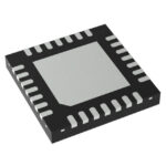 LMK1D1204PRHDT

The activity of extra discounts on wholesale prices is in full swing…
Please fill in your contact information and we will send you the latest wholesale price list.





