 ChipApex | Global Electronic Components Supplier

SEARCH
Search Product
Search Post
— IC芯片 | 连接器 | 传感器 | 被动器件 —
Search productSearch post
— IC芯片 | 连接器 | 传感器 | 被动器件 —
Consult the customer manager about the wholesale price.
consultation hotline:86-132-6715-2157
email:[email protected]
Contact the product manager for consultation. One-stop consultation is available.
Do you want a lower wholesale price? Please send us your inquiry and we will reply immediately.
LMK1D1212RHAR is listed in the Clock Buffers, Drivers range at ChipApex. The manufacturer field lists Texas Instruments. Its product description is IC CLK BUFFER 2:12 2GHZ 40VQFN. Review the specifications below when checking this part for your BOM.
The LMK1D1212RHAR is a low additive jitter LVDS buffer from Texas Instruments, packaged in a 40-pin VQFN (6-mm × 6-mm). It distributes one of two selectable clock inputs to 12 pairs of differential LVDS outputs. The device supports input frequencies up to 2 GHz and operates on a supply voltage ranging from 1.71 V to 3.465 V. Key electrical specifications include a maximum propagation delay of 575 ps, an output skew of 20 ps, and a maximum random additive jitter of 60 fs RMS at 156.25 MHz within a 12-kHz to 20-MHz integration range. It functions within an industrial temperature range of –40°C to 105°C.
Verify the RHA suffix confirms the 40-pin VQFN package with a 6.00 mm × 6.00 mm body size. Confirm the 'I' designation indicates the industrial temperature grade spanning –40°C to 105°C. Ensure the datasheet revision matches current design requirements, as pin assignments for IN0_P and IN0_N were updated in Revision A compared to earlier versions.
Select the LMK1D1212RHAR when 12 differential LVDS outputs are required from a single clock source. Use this component if the application demands high-frequency operation up to 2 GHz with minimal skew. Consider the boosted mode feature if the downstream receivers require higher voltage swings than standard LVDS provides. Verify that the power supply environment supports the 1.8-V, 2.5-V, or 3.3-V operating ranges.
This part belongs to the LMK1D121x family, which also includes the LMK1D1216 offering 16 outputs in a larger 48-pin package. Unlike the LMK1D1208 variants that offer individual output enable control, the LMK1D1212 utilizes global output enable control via pin configuration. It serves as a fan-out buffer designed specifically for driving 50-Ω transmission lines with high signal integrity.
The LMK1D1212RGZR is a pin-compatible alternative within the same family but housed in a 48-pin VQFN package containing 16 outputs instead of 12. Direct substitution requires verifying board space constraints and ensuring the unused pins are managed correctly. Other family members like the LMK1D1208 differ significantly in output count and enable control mechanisms.
Explore related parts through Clock/Timing, Integrated Circuits (ICs), all product categories, ChipApex homepage.
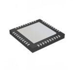 LMK1D1212RHAR

The activity of extra discounts on wholesale prices is in full swing…
Please fill in your contact information and we will send you the latest wholesale price list.






