ChipApex | Global Electronic Components Supplier
SEARCH
Search Product
Search Post
— IC芯片 | 连接器 | 传感器 | 被动器件 —
Search productSearch post
— IC芯片 | 连接器 | 传感器 | 被动器件 —
Consult the customer manager about the wholesale price.
consultation hotline:86-132-6715-2157
email:[email protected]
Contact the product manager for consultation. One-stop consultation is available.
Do you want a lower wholesale price? Please send us your inquiry and we will reply immediately.
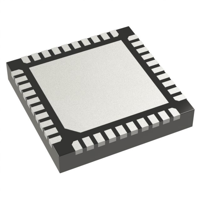
The LMKDB1108Z100RKPR is an ultra-low jitter LP-HCSL clock buffer supporting PCIe Gen 1 through Gen 7 architectures. It provides one differential input and eight differential outputs with a fixed 100Ω output impedance. The device operates on 1.8V or 3.3V supplies within the -40°C to +105°C temperature range. Key electrical specifications include a maximum additive jitter of 31fs RMS (12kHz to 20MHz at 156.25MHz) and fail-safe input functionality. It is housed in a 40-pin VQFN package.
Verify the specific suffix RKPR corresponds to the 40-pin VQFN (RKP) package and tape-and-reel delivery format. Confirm that the Z100 designation matches the required 100Ω output impedance for the target design. Ensure compatibility with the system's 1.8V or 3.3V power supply rails and SMBus interface requirements.
Select this component when designing for PCIe Gen 1 to Gen 7 interfaces requiring low jitter buffering. Choose the Z100 variant specifically for 100Ω output impedance applications; use Z85 for 85Ω loads. Consider the FS variants if fail-safe outputs are also required alongside the standard fail-safe inputs. Ensure the design accommodates the 40-pin VQFN footprint and thermal pad grounding.
This part belongs to the LMKDB11xx family of ultra-low jitter LP-HCSL buffers compliant with Intel DB2000QL specifications. While the LMKDB1120 is pin-compatible with DB2000QL, the LMKDB1108 offers a reduced channel count (8 outputs) in a smaller 40-pin VQFN package compared to the 80-pin TLGA of the 20-output variant.
LMKDB1108Z85RKPR: Identical function but with 85Ω output impedance instead of 100Ω. LMKDB1108FSZ100RKPR: Includes fail-safe outputs in addition to the standard fail-safe inputs.
 LMKDB1108Z100RKPR
The activity of extra discounts on wholesale prices is in full swing…
Please fill in your contact information and we will send you the latest wholesale price list.