ChipApex | Global Electronic Components Supplier
SEARCH
Search Product
Search Post
— IC芯片 | 连接器 | 传感器 | 被动器件 —
Search productSearch post
— IC芯片 | 连接器 | 传感器 | 被动器件 —
Consult the customer manager about the wholesale price.
consultation hotline:86-132-6715-2157
email:[email protected]
Contact the product manager for consultation. One-stop consultation is available.
Do you want a lower wholesale price? Please send us your inquiry and we will reply immediately.
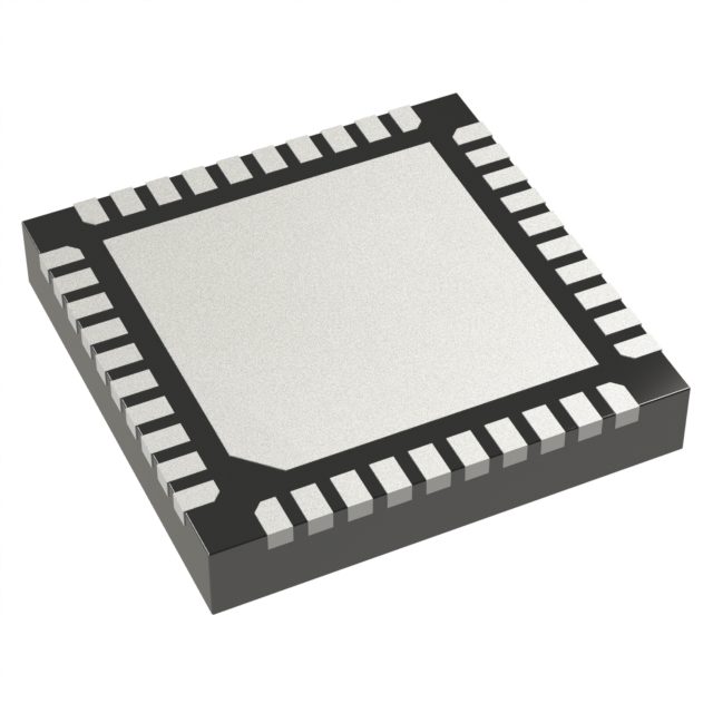
The LMKDB1108Z85RKPR is an ultra-low jitter LP-HCSL clock buffer from Texas Instruments, designed for PCIe Gen 1 through Gen 7 architectures. It features eight differential outputs with a fixed 85Ω impedance and supports both Common Clock (CC) and Independent Reference (IR) topologies. The device accepts a single differential input clock, which may include Spread Spectrum Clocking (SSC). Key electrical specifications include a maximum additive jitter of 31fs RMS (12kHz to 20MHz at 156.25MHz), with performance scaling down to 2.1fs for PCIe Gen 7. It operates on dual power supplies: 1.8V ±10% for analog circuits and 3.3V ±10% for output drivers, within an ambient temperature range of -40°C to +105°C.
Verify the specific ordering suffix 'Z85' confirms the 85Ω output impedance variant. Confirm the 'RKP' package designation corresponds to the VQFN-40 form factor. Ensure compatibility with the required 1.8V and 3.3V supply rails during component sourcing.
Select this model when eight buffered LP-HCSL outputs are required for high-speed serial links. The Z85 suffix is mandatory for designs requiring 85Ω termination. Consider the LMKDB1108FS variant if fail-safe outputs are necessary in addition to the standard fail-safe inputs provided by the Z85 version.
This component belongs to the LMKDB11xx family of PCIe clock buffers. It shares functional similarities with the LMKDB1120 and LMKDB1112 but offers a reduced channel count. Unlike the LMKDB1108FS, it lacks fail-safe outputs. It serves as a direct replacement for legacy Intel DB2000QL compliant devices in multi-channel configurations.
The LMKDB1108FS85 is a compatible alternative that adds fail-safe output capabilities. For pin-compatible replacements in existing designs, verify that the target device supports the same LP-HCSL output swing and impedance requirements.
 LMKDB1108Z85RKPR
The activity of extra discounts on wholesale prices is in full swing…
Please fill in your contact information and we will send you the latest wholesale price list.