 ChipApex | Global Electronic Components Supplier
SEARCH
Search Product
Search Post
— IC芯片 | 连接器 | 传感器 | 被动器件 —
Search productSearch post
— IC芯片 | 连接器 | 传感器 | 被动器件 —
Consult the customer manager about the wholesale price.
consultation hotline:86-132-6715-2157
email:[email protected]
Contact the product manager for consultation. One-stop consultation is available.
Do you want a lower wholesale price? Please send us your inquiry and we will reply immediately.
The LMKDB1120Z85NPPT is a low-power LP-HCSL clock buffer from Texas Instruments, designed for PCIe Gen 1 through Gen 7 architectures. It provides 20 differential outputs with an 85Ω impedance and supports both Common Clock (CC) and Independent Reference (IR) topologies. The device features extremely low additive jitter, specified at a maximum of 31fs RMS (12kHz to 20MHz) at 156.25MHz. It operates on dual power supplies: 1.8V or 3.3V ±10% for analog circuits and 1.8V or 3.3V ±10% for digital outputs. Key functional attributes include fail-safe inputs, individual output enable control, Side-Band Interface (SBI) support, and Loss of Signal (LOS) detection.
Verify that the specific ordering suffix 'NPPT' corresponds to the TLGA-80 package configuration as defined in the manufacturer's orderable information section. Confirm that the 85Ω output impedance variant matches the system design requirements, as 100Ω variants are also available within the same family.
Select the LMKDB1120Z85NPPT when a high-channel-count buffer (20 outputs) with 85Ω impedance is required for PCIe Gen 1 to Gen 7 applications. Consider the 1.8V supply option to achieve approximately 250mW lower power consumption compared to the 3.3V supply. Ensure the design accommodates the 6mm × 6mm TLGA package dimensions and thermal pad requirements.
This component belongs to the LMKDB11xx family of ultra-low jitter LP-HCSL clock buffers. The 'Z' designation indicates the 85Ω output impedance variant, while the base model LMKDB1120 provides 20 outputs. Other family members include the LMKDB1120FS (fail-safe outputs), LMKDB1112 (12 outputs), and various Mux devices.
The LMKDB1120Z85NPPT is pin-compatible with the Intel DB2000QL. For direct replacement in existing designs, verify that the replacement part maintains the 85Ω output impedance and LP-HCSL output voltage levels.
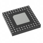 LMKDB1120Z85NPPT
The activity of extra discounts on wholesale prices is in full swing…
Please fill in your contact information and we will send you the latest wholesale price list.





