ChipApex | Global Electronic Components Supplier
SEARCH
Search Product
Search Post
— IC芯片 | 连接器 | 传感器 | 被动器件 —
Search productSearch post
— IC芯片 | 连接器 | 传感器 | 被动器件 —
Consult the customer manager about the wholesale price.
consultation hotline:86-132-6715-2157
email:[email protected]
Contact the product manager for consultation. One-stop consultation is available.
Do you want a lower wholesale price? Please send us your inquiry and we will reply immediately.
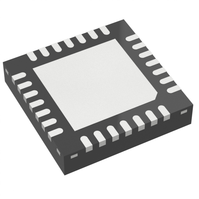
The LMKDB1202 is a low-power LP-HCSL clock multiplexer supporting PCIe Gen 1 through Gen 7 architectures. It features two differential inputs and two differential outputs with selectable 85Ω or 100Ω output impedance. The device provides extremely low additive jitter, reaching 2.1fs maximum for PCIe Gen 7 at 156.25MHz. It supports both Common Clock (CC) and Independent Reference (IR) configurations, includes fail-safe inputs, and offers individual output enable controls alongside automatic output disable functionality upon loss of signal detection.
Verify the REY suffix corresponds to the VQFN-20 package during procurement. Confirm power supply requirements match the 1.8V or 3.3V ±10% specifications. Ensure ESD handling protocols are followed due to the component's sensitivity.
Select this model when only two differential outputs are required from two input sources. Choose between 85Ω and 100Ω impedance based on the target PCB trace design. Verify that the operating temperature range of -40°C to 105°C meets the environmental constraints of the application.
This component belongs to the LMKDB12xx family, which includes the LMKDB1204 and LMKDB1208 variants. These devices share similar core functionalities but differ in the number of available outputs. The LMKDB1202 specifically provides a compact solution for applications requiring minimal output channels while maintaining ultra-low jitter performance.
LMKDB1204REX
The maximum additive jitter is 31fs RMS from 12kHz to 20MHz at 156.25MHz.
The output impedance can be selected as either 85Ω or 100Ω using the ZOUT_SEL pin.
Yes, the device supports input clocks with or without Spread Spectrum Clocking (SSC).
 LMKDB1202REYT
The activity of extra discounts on wholesale prices is in full swing…
Please fill in your contact information and we will send you the latest wholesale price list.