 ChipApex | Global Electronic Components Supplier

SEARCH
Search Product
Search Post
— IC芯片 | 连接器 | 传感器 | 被动器件 —
Search productSearch post
— IC芯片 | 连接器 | 传感器 | 被动器件 —
Consult the customer manager about the wholesale price.
consultation hotline:86-132-6715-2157
email:[email protected]
Contact the product manager for consultation. One-stop consultation is available.
Do you want a lower wholesale price? Please send us your inquiry and we will reply immediately.
The LS7216 is a CMOS integrated circuit designed for generating digitally programmable time delays. It utilizes eight binary-weighted inputs (WB0-WB7) to control the delay duration, which is determined by an applied clock or oscillator frequency. The device supports multiple operating modes including One-Shot, Delayed Operate, Delayed Release, and Dual Delay, with the output state managed via Mode Select inputs A and B. Triggering occurs through a transition at the TRIG input, while a dedicated Reset input allows for immediate delay abort. The component operates within a supply voltage range of +3V to +18V.
Verify package availability as the LS7216 is offered in both DIP and SOIC configurations. Confirm that the specific variant meets the required voltage and temperature specifications for the target application environment. Ensure compatibility with existing bus architectures if latching delay values from an 8-bit bus is intended.
Select the LS7216 when a wide dynamic range of delay times is required without complex external components. Choose this part over discrete solutions for applications needing direct relay driving capabilities. Consider the LS7215 if pinout or specific mode implementations differ slightly for the design constraints. Evaluate power supply stability given the +3V to +18V operational range.
The LS7216 belongs to the LS721x family of programmable digital delay timers manufactured by LSI Computer Systems. This series includes variants such as the LS7210, LS7211, and LS7215, which share similar core functionalities but may differ in pin counts, package types, or specific feature sets. The family is designed for general-purpose timing applications requiring reliable, long-duration delays.
Cross-reference with LS7215 for potential functional equivalence, noting any differences in package or specific mode support. Verify pin-to-pin compatibility before substitution to ensure proper integration into existing PCB layouts.


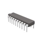 LS7216

The activity of extra discounts on wholesale prices is in full swing…
Please fill in your contact information and we will send you the latest wholesale price list.



