ChipApex | Global Electronic Components Supplier

SEARCH
Search Product
Search Post
— IC芯片 | 连接器 | 传感器 | 被动器件 —
Search productSearch post
— IC芯片 | 连接器 | 传感器 | 被动器件 —
Consult the customer manager about the wholesale price.
consultation hotline:86-132-6715-2157
email:[email protected]
Contact the product manager for consultation. One-stop consultation is available.
Do you want a lower wholesale price? Please send us your inquiry and we will reply immediately.
LT1884AIN8#PBF is listed in the Instrumentation, Op Amps, Buffer Amps range at ChipApex. The manufacturer field lists Analog Devices Inc.. Its product description is IC OPAMP GP 2 CIRCUIT 8DIP. Review the specifications below when checking this part for your BOM.
The LT1884AIN8#PBF is a dual precision operational amplifier featuring rail-to-rail output swing and picoampere input bias currents. It operates on supply voltages between 2.7V and 36V, with full specification from 5V to ±15V. The device offers an input offset voltage of 50mV maximum, low drift of 0.8mV/°C, and a gain-bandwidth product of 2MHz. Supply current per amplifier is less than 1mA, supporting low-power applications while maintaining high accuracy.
Verify the specific 'A' grade designation ensures the tighter offset voltage and bias current specifications compared to standard variants. Confirm the N8 suffix corresponds to the 8-lead PDIP package required for your assembly process. Ensure the datasheet revision matches the design requirements for temperature range and electrical characteristics.
Select this component when both high DC precision and AC speed are required in a low-power environment. The rail-to-rail output allows for maximum dynamic range in single-supply designs. Consider the input bias current cancellation circuit which requires minimal external impedance balancing for optimal performance.
This part belongs to the LT1884/LT1885 family of dual and quad precision op amps. It combines the low noise and bias current typical of bipolar inputs with the output swing capabilities of CMOS stages. The family addresses the need for precision in battery-operated and portable instrumentation where power consumption must be minimized without sacrificing signal integrity.
LT1884CN8#PBF
The internal cancellation circuit makes the input bias currents uncorrelated. Therefore, unlike JFET amplifiers, external resistance balancing at the input pins is not recommended and may increase error.
The input stage operates between VEE + 0.8V and VCC – 0.9V. Exceeding this range causes the gain to drop to zero but does not result in phase reversal.
Explore related parts through Amplifiers, Linear, Integrated Circuits (ICs), all product categories.
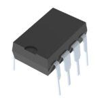 LT1884AIN8#PBF

The activity of extra discounts on wholesale prices is in full swing…
Please fill in your contact information and we will send you the latest wholesale price list.