 ChipApex | Global Electronic Components Supplier
SEARCH
Search Product
Search Post
— IC芯片 | 连接器 | 传感器 | 被动器件 —
Search productSearch post
— IC芯片 | 连接器 | 传感器 | 被动器件 —
Consult the customer manager about the wholesale price.
consultation hotline:86-132-6715-2157
email:[email protected]
Contact the product manager for consultation. One-stop consultation is available.
Do you want a lower wholesale price? Please send us your inquiry and we will reply immediately.
The LT1993IUD-10#PBF is a low distortion, low noise differential amplifier and ADC driver from Analog Devices Inc. It features a fixed gain of 20dB (10V/V) and a -3dB bandwidth of 700MHz. The device operates on a single 5V supply with typical current consumption of 100mA. It includes built-in 175MHz differential lowpass filtering accessible via dedicated filtered outputs. The component is housed in a compact 16-lead 3mm x 3mm QFN package.
Verify that the ordering suffix #PBF confirms lead-free status and RoHS compliance as specified by the manufacturer. Ensure the temperature grade 'I' matches the required operating range of –40°C to 85°C. Confirm the package type is the 16-lead 3mm x 3mm QFN. Cross-reference the datasheet revision to ensure pinout and electrical characteristics align with your design specifications.
Select this component when a fixed 20dB gain and wide 700MHz bandwidth are required for signal conditioning. It is suitable for applications needing integrated anti-aliasing filtering without additional external components. Consider the 5V single-supply requirement and 100mA current draw during power budgeting. Verify that the input impedance and drive capabilities meet the source and load requirements of the target ADC or receiver stage.
This part belongs to the LT1993 family of differential amplifiers designed specifically for driving high-speed ADCs. The 'I' suffix denotes an industrial temperature range, while 'UD' indicates the specific 16-lead QFN package. The '#PBF' suffix signifies a lead-free finish compliant with environmental standards. This variant provides a balance of performance and integration for communication transceiver applications.
Consult official documentation for confirmed substitutes. No public substitute part numbers are verified in the provided source material.
The VOCM pin sets the output common mode voltage. Without additional biasing, it also biases the inputs to this voltage, allowing direct coupling to ADCs without transformers.
The ENABLE pin is a TTL logic input referenced to VEEC. A low voltage enables the device with typical 100mA current draw, while a high voltage disables it, reducing current to approximately 250µA.
The unfiltered outputs (+OUT, –OUT) provide full bandwidth up to 700MHz. The filtered outputs (+OUTFILTERED, –OUTFILTERED) include an internal 175MHz lowpass filter formed by series resistors and capacitors.
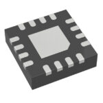 LT1993IUD-10#PBF
The activity of extra discounts on wholesale prices is in full swing…
Please fill in your contact information and we will send you the latest wholesale price list.





