 ChipApex | Global Electronic Components Supplier
SEARCH
Search Product
Search Post
— IC芯片 | 连接器 | 传感器 | 被动器件 —
Search productSearch post
— IC芯片 | 连接器 | 传感器 | 被动器件 —
Consult the customer manager about the wholesale price.
consultation hotline:86-132-6715-2157
email:[email protected]
Contact the product manager for consultation. One-stop consultation is available.
Do you want a lower wholesale price? Please send us your inquiry and we will reply immediately.
The LT6108AHMS8-1#PBF is a high-side current sense amplifier featuring an integrated comparator and voltage reference. It operates within a supply voltage range of 2.7V to 60V with a typical supply current of 450µA. The device incorporates a precision current sense amplifier with a maximum input offset voltage of 125µV and a bandwidth of 1MHz. The internal comparator provides a latching output with a threshold error of ±1.25% and a propagation delay of typically 1.4µs. It is housed in an 8-lead MSOP package and specified for operation from –40°C to 125°C.
Verify the specific suffix 'AH' indicates the extended temperature grade (-40°C to 125°C) and 'HMS8' denotes the 8-lead MSOP package. Confirm the '-1' suffix corresponds to the version with the latching comparator. Ensure compatibility with the required supply voltage range and check for lead-free finish specifications if mandated by project requirements.
Select this component when high-side sensing is required with integrated fault protection. The latching comparator option is suitable for applications needing persistent fault flags until reset. Consider the 125µV maximum offset voltage for low-current accuracy needs. Verify that the external gain resistors can be selected to maintain the output current within the 1mA limit while achieving the desired voltage swing.
This part belongs to the LT6108 family of high-side current sense amplifiers. The LT6108-1 variant specifically includes a latching comparator, distinguishing it from the non-latching LT6108-2. The 'A' grade offers tighter electrical specifications compared to standard grades, ensuring higher precision in offset voltage and gain error across the operating temperature range.
LT6108AHMS8-2#PBF (Non-latching comparator version)
The LT6108-1 features a latching comparator that holds the output state after a fault event until explicitly reset via the EN/RST pin. The LT6108-2 has a non-latching comparator that returns to its normal state once the fault condition is removed.
The gain is set by two external resistors: RIN connected between V+ and SENSEHI, and ROUT connected between OUTA and V–. The voltage gain is determined by the ratio of ROUT to RIN.
Yes, the comparator trip point is configured using external resistors. The internal 400mV reference serves as one input to the comparator, while the other input is connected to a voltage divider derived from the amplifier's output.
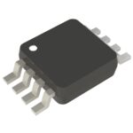 LT6108AHMS8-1#PBF
The activity of extra discounts on wholesale prices is in full swing…
Please fill in your contact information and we will send you the latest wholesale price list.







