 ChipApex | Global Electronic Components Supplier
SEARCH
Search Product
Search Post
— IC芯片 | 连接器 | 传感器 | 被动器件 —
Search productSearch post
— IC芯片 | 连接器 | 传感器 | 被动器件 —
Consult the customer manager about the wholesale price.
consultation hotline:86-132-6715-2157
email:[email protected]
Contact the product manager for consultation. One-stop consultation is available.
Do you want a lower wholesale price? Please send us your inquiry and we will reply immediately.
The LT6108IDCB-1 is a high-side current sense amplifier with an integrated comparator and reference, housed in an 8-lead DFN package. It operates within a supply voltage range of 2.7V to 60V and supports a specified temperature range of –40°C to 85°C. The device features a maximum input offset voltage of 350µV and a gain error of 0.2% maximum. It includes a latching comparator with a typical threshold of 400mV and a total threshold error of ±1.25%. Supply current is typically 450µA, reducing to 5µA maximum in shutdown mode.
Verify the specific ordering suffix IDCB-1#TRMPBF against official Analog Devices documentation to confirm the 8-lead DFN package and tape-and-reel quantity. Ensure the temperature grade matches the required operational environment. Confirm lead-free finish compliance if necessary for assembly processes.
Select this component when a high-side sensing solution with integrated fault protection is required. The latching comparator option distinguishes it from non-latching variants. Consider the thermal performance of the DFN package for high-voltage applications where exposed pad connection may be utilized for improved heat dissipation.
This part belongs to the LT6108 family of high-side current sense amplifiers. It shares core functionality with MSOP-packaged versions but utilizes a compact plastic DFN form factor. The -1 suffix indicates the inclusion of a latching comparator, differentiating it from the -2 variant which offers a non-latching output.
LT6108HDCB-1#TRMPBF (Higher temperature grade)
The EN/RST pin serves as both the enable input and the latch reset input. Pulling it low for a specific duration resets the latching comparator state.
The gain is set by external resistors RIN and ROUT. The output current is proportional to the sense voltage divided by RIN, and converted to voltage by ROUT.
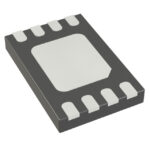 LT6108IDCB-1
The activity of extra discounts on wholesale prices is in full swing…
Please fill in your contact information and we will send you the latest wholesale price list.





