ChipApex | Global Electronic Components Supplier
SEARCH
Search Product
Search Post
— IC芯片 | 连接器 | 传感器 | 被动器件 —
Search productSearch post
— IC芯片 | 连接器 | 传感器 | 被动器件 —
Consult the customer manager about the wholesale price.
consultation hotline:86-132-6715-2157
email:[email protected]
Contact the product manager for consultation. One-stop consultation is available.
Do you want a lower wholesale price? Please send us your inquiry and we will reply immediately.
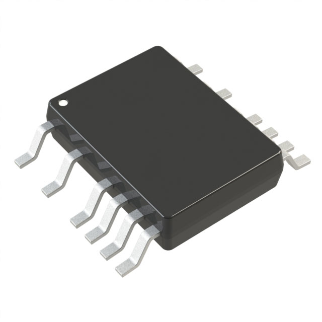
The LT8364IMSE#PBF is a current mode DC/DC converter featuring an internal 4A, 60V switch. It operates from a 2.8V to 60V input range and supports boost, SEPIC, or inverting topologies. The device offers a programmable switching frequency between 300kHz and 2MHz. It utilizes Burst Mode operation to achieve a quiescent current of 9μA while maintaining output ripple below 15mVP-P. The component is housed in a 16-lead MSOP package with an exposed pad and is rated for industrial temperatures from -40°C to 125°C.
Verify the specific suffix #PBF indicates lead-free compliance and RoHS adherence. Confirm the IMSE designation corresponds to the industrial temperature grade (-40°C to 125°C) and the 16-lead MSOP package variant. Ensure the ordering part number matches the exact manufacturer specification sheet to avoid confusion with other thermal grades or package options within the LT8364 family.
Select this component when designing circuits requiring wide input voltage ranges up to 60V with high peak current capabilities. The adjustable frequency feature is critical for applications needing to bypass sensitive RF bands or optimize magnetic component sizes. Consider the exposed pad thermal performance for high-duty cycle operations and verify that the 4A switch rating aligns with the maximum inductor current requirements of the target topology.
This part belongs to the LT8364 family of low IQ converters manufactured by Analog Devices. It shares core functionality with variants like the LT8364EDE and LT8364HDE but differs in package type and thermal rating. The IMSE version specifically targets industrial environments requiring robust performance across extended temperature ranges compared to commercial grade alternatives.
Direct substitutes include LT8364EMSE#PBF (commercial temp), LT8364IDE#PBF (DFN package), and LT8364HDE#PBF (high temp DFN). Verify pin compatibility and thermal characteristics when swapping between MSOP and DFN packages within the same family.
The device employs Burst Mode operation which reduces quiescent current to 9μA and maintains typical output ripple below 15mVP-P even at very low output currents.
The BIAS pin accepts a second input voltage to supply the INTV regulator, which increases overall system efficiency by reducing power dissipation within the IC.
 LT8364IMSE#PBF
The activity of extra discounts on wholesale prices is in full swing…
Please fill in your contact information and we will send you the latest wholesale price list.